
Abstract: Due to the internal structure of synchronous dynamic random access memory SDRAM, its control logic is more complicated. Field programmable logic gate array FPGA as a semi-custom circuit has the advantages of fast speed, rich internal resources and reconfigurability. In this paper, an FPGA-based SDRAM controller is designed. Based on the logic structure of the controller, the data communication between FPGA and SDRAM is analyzed. The SDRAM is equipped with automatic pre-charge burst read and write and non-automatic pre-processing. Charge the entire page to read and write.
0 Preface
SDRAM (Synchronous Dy namic Random Access Memory) has the advantages of low price, large capacity, and high speed. However, the control logic of SDRAM is relatively complicated, and the timing requirements are strict. This requires a special controller. The FPGA (Field Programmable Gate Array) features high speed, multiple interfaces, and reconfigurability. The FPGA-based SDRAM controller design can greatly shorten the development cycle and simplify the design method. In the past, there were many articles on the design of SDRAM controllers, but the accuracy of reading and writing data was rarely considered from the perspective of FPGA timing analysis. This paper applies FPGA to build SDRAM controller, and performs timing analysis on FPGA and SDRAM construction models to complete functional simulation. And timing simulation, and finally achieve normal read and write of SDRAM through board level debugging.
1. 1 Introduction to SDRAM
The function pins of SDRAM can be divided into three types: control signal, address signal and data signal.
The control signals mainly include a chip select signal, a clock signal, a clock enable signal, a row and column address selection signal, a read/write signal, and a data valid signal.
The address signals are divided into block addresses, row addresses, and column addresses, where the row and column addresses are time-multiplexed. The row address is latched when the row activates the command, and the column address is latched when the command is read or written.
The data signal is a bidirectional signal to reduce pin connections and is controlled by data valid signals.
SDRAM requires an initialization process before it can work properly:
(1) Wait for 200us after power-on to stabilize the power and clock signals.
(2) Pre-charge all BANKs in the SDRAM to prepare the memory array in the device.
(3) Complete at least 8 auto-refresh operations to make the internal SDRAM refresh and counters in normal operation.
(4) Configure the working mode register.
SDRAM should periodically perform automatic refresh operation to ensure that internal data will not be lost. Currently, the recognized line refresh period is 64ms, which can be either centralized or decentralized. SDRAM has a refresh address counter. Each time the auto refresh counter is completed, it will be added automatically. 1.
SDRAM read and write can be set by burst configuration and burst type.
The burst read and write length is 1, 2, 4, 8 or full page mode. The pre-charged burst read and write can be implemented by setting the 10th bit of the address bit when the read/write command is valid. The precharge command can be used to end the current active line operation. For normal burst read and write, only the first row activation is performed in the same row operation, and the column address can be written in several subsequent operations. To switch between different lines, you first need to pre-charge to close the current active line, and then activate the next line of operation in the execution line activation command. The burst read and write with pre-charge automatically restarts the current active line after each operation is completed. Therefore, each time the read and write is performed, the line is activated first and then the read/write command is issued.
The full page read/write mode can read and write any length of the entire page. The maximum length is 256. After each read and write is completed, a burst termination command is required to end the reading and writing. The charge command closes the current line.
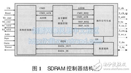
1. 2 SDRAM controller structure system adopts modular design and can be divided into 4 modules, as shown in Figure 1, including system control interface module, command parsing and refresh control module, operation signal generation module and data path module. The system control interface module mainly completes the initialization work by the state machine and generates the CMD command; the command parsing and refresh control module mainly issues the command request of the CMD to issue a command request and simultaneously issues a refresh request according to the refresh counter; the operation signal generating module generates the arbitration request by the arbiter. Command signals are sent to the SDRAM device; the data path module controls the direction of data stream transmission and produces efficient data input and output.
1. 3 module design
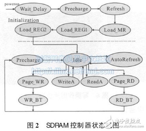
1. 3. 1 System Control Interface Module This module implements SDRAM initialization and control command generation functions through the state machine. Figure 2 shows the state machine diagram. The SDRAM initialization process mainly includes: 200u wait time is generated by the counter after the system is powered on, secondly, a precharge command is executed, then 8 self-refresh operations are completed, and finally the register is configured.
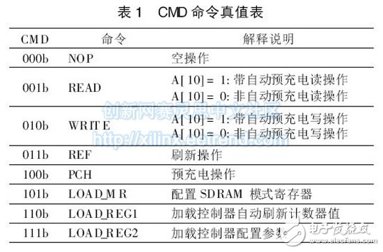
The control interface module generates a CMD command according to the receiving external command and the back-end module response signal, and sends the CMD command to the back-end module for corresponding operation. Table 1 is the CMD signal truth value table.
1. 3. 2 Command Parsing and Refresh Control Module This module mainly decodes the CMD command into the next module. Only one command request output is allowed at the same time. The controller parameter configuration value and the refresh counter value are loaded into the internal registers during register configuration. At this time, the refresh control module starts counting, and when the preset value in the register is reached, a refresh request is issued, and when the response is refreshed, the counter continues to work, and the cycle is repeated.
1. 3. 3 Operation Signal Generation Module This module first receives the command request and the refresh request. The arbiter sends the SDRAM corresponding operation signal to the SDRAM through the arbiter according to the principle that the refresh request priority is higher than the command request. At the same time, the module generates a data enable signal OE to the data path module to control the data flow.
Since the SDRAM address signals are time-multiplexed, the address signal ADDR of the controller is the block address, row address, and column address of the SDRAM from high to low. In this module, the block, row, and column addresses contained in the ADDR are written into the response register. When the row is activated, the block address and the row address are sent to the SDRAM, and the column address is sent to the SDRAM when the read/write command is issued.
1. 3. 4 Data Path Module This module mainly handles the operation of the data path during the read and write operations. The OE signal is used as the tri-state gate enable terminal. When the write operation is high valid data, the DATAIN is written to the SDRAM via the SDRAM bidirectional data line DQ. ; OE is low data read from DQ to the FPGA internal DATAOU T data bus during a read operation. DQM is the data mask. When DQ is 16 bits, the DQM width is 2. By setting the value of different bits of DQM, the DQ bit can be read and written by 8 bits. At the same time, the value of DQM can be set by setting the DQM value at different reading and writing times. SDRAM read and write operations at any address.
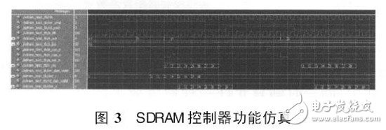
2 Simulation verification2. 1 Functional Simulation After the controller design code is completed, functional logic simulation is first performed to check whether the design syntax is correct and whether the design function is fully implemented. The test vector must be written in a complete manner, and the design working mode of SDRAM should be considered.
Figure 3 shows the functional simulation of the controller. At this time, the burst length is 8, the tRCD delay is 3 clocks, and the tCAS delay is 3 clocks. After the write command is issued, the data is written into the SDRAM when the write data enable signal is asserted; after the read command is issued, the data is read from the SDRAM when the read data enable signal is asserted.
2. 2 Timing Simulation Timing simulation is a simulation process that reverses the device delay and wiring delay to the simulation file after designing the integrated layout and routing. The timing simulation is closer to the actual behavior of the device. Timing analysis is first performed in the timing simulation stage. If the timing requirements of the signal are not met, the corresponding timing constraints are added, and the simulation is verified again to ensure that all signals can be correctly written and read.
2. 2. 1 Timing Analysis Since the SDRAM pin signals are valid on the rising edge of the clock signal, it is known from the SDRAM data sheet that each signal establishes the hold time. Data signals that also enter the FPGA from SDRAM must also meet the FPGA setup hold time.
Figure 4 shows the FPGA and SDRAM data transfer models, where:
T din is the transfer time of data from the IO port of the FPGA to the internal register;
T 0co is the data transfer time in the FPGA internal register;
T out is the transfer time of data from the output of the FPGA register to the IO port;
T pcb is the data trace time on the PCB board;
T 1co is the data transfer time in the SDRAM internal register.
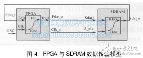
Assume that all signals are equal in PCB trace delay. The external clock source enters the FPGA through the global clock network while outputting the clock signal from the FPGA to the SDRAM. The zero-phase offset of clk and s_clk can be achieved by setting the clock management unit DCM.
When SDRAM is used as a downstream device of the FPGA, the data signal entering the SDRAM needs to meet the setup hold time on the rising edge of the clock. As shown in Figure 5, when SSetup and SHold respectively satisfy the data setup and hold time in SDRAM, the data will be correctly written into SDRAM. If the requirement is not met, since T0co is generally fixed according to the specific device, it can be properly constrained. Tout time to meet timing requirements.
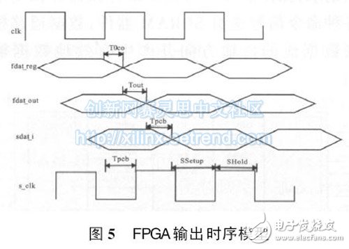
When SDRAM is used as an upstream device of the FPGA, the data signal entering the FPGA must also meet the setup hold time on the rising edge of the clock. If it is not met, the time requirement can be met by timing constraint data from the IO of the FPGA to the internal register transfer time Tdin.
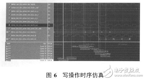
2. 2. 2 Timing Simulation and Verification Figure 6 shows the timing simulation of the SDRAM controller write operation. It can be seen from the waveform that the clock period Tclk= 10000ps, SSetup=1763ps, SHold= 6799ps. Check the SDRAM data sheet to see that the setup hold time is met.
After the simulation is completed, the generated download file is loaded into the FPGA, and the test logic is added to make the unobservable data in the SDRAM ensure correct reading and writing by, for example, LED display. At the same time, you can quickly detect and locate problems with the online logic analyzer ChipScope.
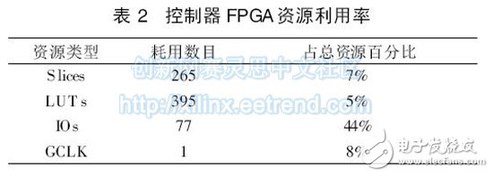
4 Conclusion and analysisThe design development environment is ISE12. 2, and the simulation environment is Modelsim6.5. The FPGA device is the XILINX-SPARTAN3 -XC3S400 with a speed class of -4. The SDRAM model is HYNIX-HY57V641620FTP-6. Table 2 lists the resource utilization of the controller; the system clock speed can reach 100MHz in terms of read and write bandwidth, and Table 3 shows the effective bandwidth of reading and writing in various modes at 100MHz.
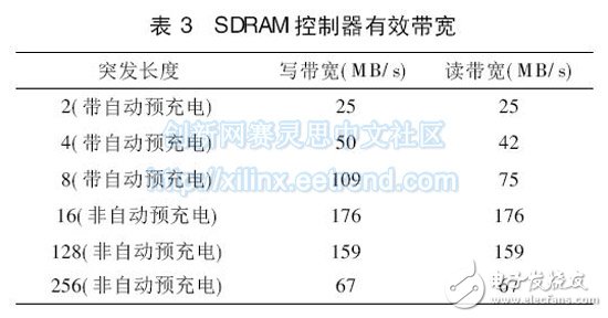
Since the read and write operation with precharge is performed, the SDRAM will be automatically precharged after each operation, which is equivalent to closing the current active line. Even if it is the same line operation, the line activation command must be executed first, and then the read operation is performed. Write commands, which affect the effective bandwidth of SDRAM to some extent. The entire page is read and written once for each pre-charge. As the burst length increases, some command operations and wait times are reduced, and the bandwidth is greatly increased.
In this paper, the SDRAM controller is designed according to the development process of FPGA, and the timing analysis of FPGA and SDRAM data interface is carried out, and the timing simulation is carried out. Board-level verification ensures the correctness of the design. This controller can work in different modes according to the setting of parameters, and has certain versatility.
Bitcoin mining machines are one way to obtain bitcoins. Bitcoin is an online virtual currency created by open-source peer-to-peer software. Instead of being issued by a specific currency institution, and produced by the massive computation of a specific algorithm, the Bitcoin economy uses a distributed database of nodes throughout the P2P network to identify and record all transactions. The decentralized nature and algorithm of P2P can ensure that it is impossible to artificially manipulate the value of bitcoin by producing a large number of coins.
Any computer can become a mining machine, but the returns will be low, and it may not mine a single bitcoin in a decade. Many companies have developed specialized Bitcoin mining machines with special mining chips that are tens or hundreds of times faster than normal computers.
Currency system by the user (the user through the key control wallet), trade (trade will be broadcast to the whole currency network) and miners (generated by competition calculation agreed on each node of the chain block, block chain is a distributed public authority books, contains the currency network of all the transactions happened)
Bitcoin miners manage the Bitcoin network by solving the problem of proof-of-work mechanisms with a certain amount of work -- confirming transactions and preventing double payments. Because hashing is irreversible, finding the number of random adjustments required to match is difficult, requiring a trial-and-error process that can predict the total number of times. This is where the proof-of-work mechanism comes into play. When a node finds a solution that matches the requirement, it can broadcast its result to the whole network. Other nodes can then receive the newly solved data block and check whether it matches the rule. If the other nodes calculate the hash value and find that the requirement (the operation goal required by Bitcoin) is satisfied, then the data block is valid and the other nodes accept the data block.
Bitcoin Mining Machine:S19 Pro Hyd Asic Miner,S19 Pro Hyd Antminer Bitmain,S19 Hyd Bitmain Antminer,s19j pro antminer bitmain,whatsminer m50s,etc.
Bitcoin Mining Machine,Antminer S19j Pro,bitcoin Miner,btc mining machine,S19 Pro Hyd
Shenzhen YLHM Technology Co., Ltd. , https://www.sggminer.com