1 Introduction
In the motor drive, UPS and other systems, voltage stability is particularly important. Undervoltage and overvoltage protection are essential. Therefore, the reliability and safety of the power supply are improved by integrating overvoltage and undervoltage protection circuits inside the chip. For power integrated circuits, to improve the reliability of the circuit, the protection circuit is also essential. The design of the protection circuit should be simple and practical. This paper designs an undervoltage protection circuit under CMOS technology. This circuit is simple in structure and easy to implement. It can be used as a power protection circuit for high voltage or power integrated circuits.
2. Analysis of working principle
The circuit schematic of undervoltage protection is shown in Figure 1. It consists of five parts: bias circuit, reference voltage generation, undervoltage detection input, comparator, and feedback loop.
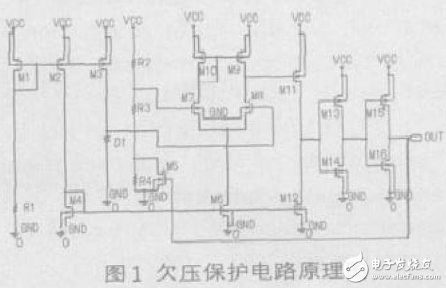
The power supply voltage of this circuit is 15V, M1, M2, M4, and R1 are the offset parts of the circuit, which provides bias to the latter circuit. The resistor R1 determines the operating point of the circuit. M1, M2, and M4 are current mirrors; M3, D1 generates the reference voltage and inputs the non-inverting terminal of the comparator; the voltage dividing resistors R2, R3 and R4 are the undervoltage detection input and input to the inverting terminal of the comparator; R4 and M5 are the feedback loops of the undervoltage signal; the remaining M6~M16 are composed. Four-stage amplification comparator.
M3, D1 generate the reference voltage, input to the non-inverting terminal of the comparator, fixed at 11V. When the power supply voltage works normally, the undervoltage detection of the inverting terminal is higher than 11V, and the comparator output is low. When M5 is cut off, the feedback circuit does not work; when the undervoltage occurs, the voltage dividing resistors R2, R3, and R4 reflect relatively sensitive. When the resistor is divided, the voltage input to the inverting terminal is less than 11V, and the output voltage of the comparator is high. This signal turns M5 on, so that the voltage across R4 becomes the saturation voltage across M5, approaching 0V, which further lowers the output voltage after R2 and R3 voltage division, forming a positive feedback of undervoltage. The output is high and undervoltage lockout protects the output.
3. Parameter calculation
For MOS analog integrated circuits, the operating state and tube size and width-to-length ratio of each MOS transistor determine the function and performance of the circuit. The following is a combination of 0.6μm process to estimate the resistance of the circuit and the width-to-length ratio of each tube. Set the total power consumption of the circuit Pm "3mW, VCC is 15V, and Uth is approximately 1V. The total current is available based on the total power consumption:

The circuit has eight loops (200/8), which can roughly distribute the current of each channel by about 20 μA: so the bias current is 20 μA, that is, the resistance of the resistor R1 is approximately

The MOS tube in the circuit works in the saturation region, and the formula of the saturation region of the MOS transistor:

The width-to-length ratio of M1 can be estimated, and the relationship between the width-to-length ratio of the current mirror and the PMOS and NMOS and the mobility

The ratio of M2, M3, M4 can be obtained, namely:

The voltage value of the Zener diode should be set in consideration of the realization of the process and should be selected under the condition that the M3 operation is in the saturation region, where the voltage value is selected as 11V; and the design of the resistor should consider the area factor. Resistors R2, R3, and R4 form a voltage divider. Set the current in this path to 30 μA, ignoring the resistance of M5.
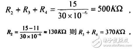
Among them, R3=300KΩ, R4=70KΩ
The gain of the comparator should be large enough to set the open-loop gain of the comparator above 80dB (104 times), since the actual fabricated product tends to be much smaller than the theoretically calculated magnification. Therefore, we assign the magnifications of each level: Aμ1=50, Aμ2=20, Aμ3=10. The total magnification is the product of the magnifications of each level, which is:

The four-way sum of the currents assigned to each stage does not exceed 110 μA (200 μA-20 & TImes; 3 μA - 30 μA). Therefore, the currents assigned to each stage are 30 μA, 20 μA, 30 μA, and 30 μA, respectively. In this way, we can calculate the width to length ratio of each tube based on the magnification and bias current.
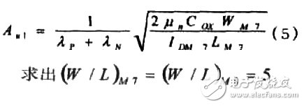
For differential amplification stages. The amplification factor Aμ1=50, the bias current is 30μA, and the current of the two branches is 15 μA. According to the calculation formula:
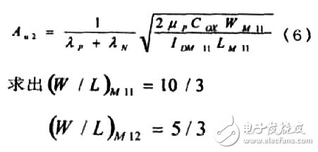
The second level, the common source amplification stage. Magnification A μ2=20, current flowing through 20 μA, according to
The third and fourth stage push-pull CMOS amplification stages, by the formula:
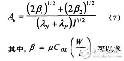
The width to length ratio of each tube from M13 to M15 is:

The calculation of the width-to-length ratio of the active load tube of the differential pair. From the voltage point of view, in order to ensure that all the tubes work in the constant current region or the critical constant current region in the signal range without entering the deep linear region, according to the total power supply voltage VDD = 15V, we can roughly assign the static of M9, M10. . then:
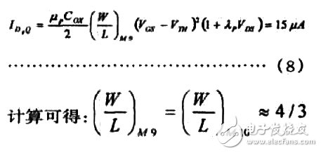
The calculation is available:

Led Street Lamps,Led Solar Street Lamps,Led Lighting Street Lamps,Led Integrated Solar Street Light
Jiangsu Bosiwei Optoelectronics Group Co.,ltd , https://www.bswledled.com
