
The Chinese government's "13th Five-Year Plan" draft, economic development goals include advanced industries such as semiconductors and the world's leading in the next generation of wafer materials, robotics, aerospace equipment and satellites, research and development funding will reach 2.5% of GDP.
So how is semiconductor made? Here we are not exploring the process from sand to chip, but focusing on the environment and production equipment for semiconductor manufacturing.
The production of semiconductor chips usually goes through the following processes:

Semiconductor chip production process
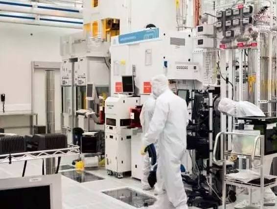
These high-end and fine preparation processes are extremely demanding on the production environment and equipment requirements of the chip. These machines will cause silicon chips (such as Intel silicon chips) to be subjected to ultra-high vacuum processing, "chemical bath" immersion, high-energy plasma processing, and ultraviolet light. A series of steps such as light irradiation, and at the same time, the silicon chips are passed through hundreds of manufacturing stages, thereby turning them into CPUs, memory chips, graphics processors, and the like. Let's take the example of the semiconductor production environment and preparation equipment of American Applied Materials' Metan Technology Center.
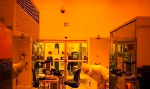
Clean room

Before entering the research center, you must wear protective clothing, masks, goggles, two gloves, and a plastic bag that completely covers the shoes. This is not a production shop. Instead, the clean room only simulates the fab environment. Applied Materials' equipment will be used in this environment so that the company and its customers can test new technologies and processes and then truly Pushed to the production line.
2. Glass photomask
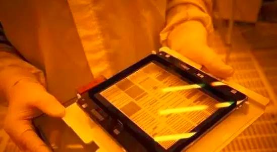
The core technology of chip manufacturing is lithography (lithography). This technology is like screen printing, except that the ink is not pressed onto the cotton T-shirt by the silk template, but by the glass photomask. The light-irradiated surface is coated on a silicon substrate coated with a photoresist (an organic compound). Where the UV light penetrates, the chemical properties of the photoresist are attenuated, leaving a pattern on the surface of the silicon chip. The silicon chip is then fed into a "chemical bath" where the trench is etched on the exposed silicon substrate while the area covered by the photoresist is not affected. After the photoresist is removed, other devices fill the trenches with a variety of materials, such as copper or aluminum used to make processor parts. This figure shows a photomask with a pattern printed on the silicon chip.
3.Technical first-class machinery and equipment
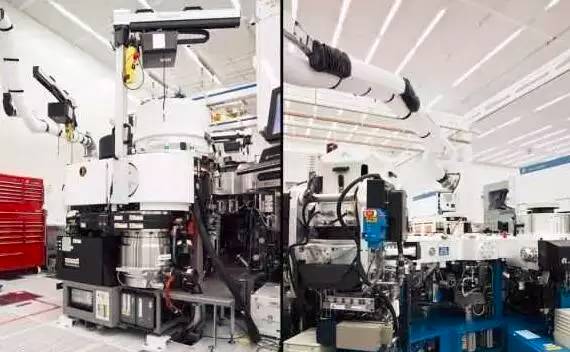
As the silicon chip is sent to the manufacturing floor, it will be processed through as many as 250 different steps. These steps include coating a variety of materials with a thin film followed by etching to form transistors and copper wires. The picture on the right is the Endura machine. The Endura platform is a modular, configurable system for mounting metals and metal alloys to silicon chips. The left picture shows the Tetra III advanced mask etching system. All mask manufacturers around the world use this system to develop and produce masks with a diameter of 45 nanometers.
4. Flatbed printing room
The chip diameter manufactured according to the current state of the art is 30 nanometers, that is, the average size of chip components is about 30 billionths of a meter. Chip makers are currently developing chip designs with a diameter of 22 nanometers, which will result in smaller chip components. Some parts are much thicker than the width, and sometimes this ratio is 60 to 1, further increasing the difficulty of chip manufacturing. This means that the etching system must be able to engrave extremely deep, extremely narrow grooves on the chip with ultra-high precision on a nanometer scale. A yellow light is placed inside the lithographic printing chamber to prevent the photomask from interfering with the ultraviolet light.
5. Extreme vacuum state
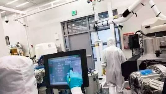
Technicians work on the touch screen interface of the Endura system. The picture shows a large silver pump used to create an extreme vacuum in the machine – as low as 10-12 atmospheres. In contrast, the altitude of 124 miles (about 200 kilometers) from the ground (the location of the space shuttle flight orbit) is 10-10 atmospheres.
6. Front-mounted wafer transfer box
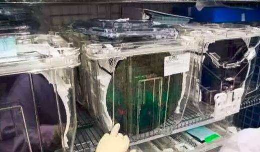
Silicon chips used to make chips have steadily increased in size over the past few decades, allowing manufacturers to integrate more chips per disk. Since 2000, the industry standard for silicon chip diameter has been 300 mm. To simplify the transfer process and minimize the risk of contamination, the fab will take advantage of the front-mounted wafer transfer cassette (FOUP). Each front-mounted wafer cassette can hold 25 silicon chips in a sterile, clean environment. Then, the machine inhales the silicon chips inside, and automatically processes them one by one.
7. Highly automated
The front-mounted wafer transfer cassette filled with silicon is very heavy, about 9 kg, and automation has become an important part of the clean room design. The clean room has an automated suspension monorail that transports the front-mounted wafer cassette from one location to another. Up to 700 front-mounted wafer cassettes (loading 17,500 silicon chips) can be placed in the sealed room shown in the photo. The robotic arm moves them in and out from both sides, placing them on a suspended monorail that runs through the entire clean room (not shown on this photo).
An additional 2,800 front-mounted wafer cassettes can be stored in a layer below the main clean room. Every machine in a modern clean room is designed and built around a 300 mm silicon chip. The new generation of chips will be fabricated on 450mm silicon chips for greater economies of scale. However, to be compatible with 450mm silicon chips, the entire industry must replace every piece of equipment.
8. Precise manufacturing of components
Although computer chips are only about the size of fingernails, they are made up of hundreds of millions of transistors, and the wiring used to connect these transistors to the machine and connect the machine to the motherboard and the rest of the world is like a labyrinth. The chips are all made of round silicon chips approximately 1 foot in diameter (about 30 cm), each of which can contain 200 separate, but identically shaped processors. Due to occasional contamination incidents, although the clean room is extremely clean, the manufacturer must still test every component of those processors to ensure that 500 million parts (each about 30 to 45 nanometers in diameter) are in the manufacturing process. There will be no embarrassment. Therefore, the cost of such machines is hundreds of billions of dollars. A mature fab that can hold hundreds of these machines costs billions of dollars.
European Socket Connector,Straight Needle European Socket Connector,Waterproof European Socket Connector,Vertical Straight European Socket Connector
Shenzhen Jinyicheng Electronci Technology Co.,Ltd. , https://www.jycconnector.com