
With the rapid development of large-scale integrated circuits and single-chip microcomputers, complex programmable logic devices (CPLDs) have the advantages of flexible use, high reliability, and powerful functions, and have been widely used in electronic product design. CPLD can be programmed in the system, repeated many times, and is also compatible with the IEEE1149.1 (JTAG) standard test excitation and boundary scan capabilities. Using CPLD devices for development can not only improve system integration, reliability and scalability. Sex, and greatly shorten the design cycle of the product. Since the CPLD uses a continuous connection structure, it is easy to predict the delay, which makes the circuit simulation more accurate. CPLDs are standard LSI products that can be used in the design of various digital logic systems. In recent years, with the adoption of advanced integration processes and mass production, the cost of CPLD devices has been declining, integration density, speed and performance have been greatly improved, so that a chip can realize a complex digital circuit system; The development tools bring great convenience to design changes. This article takes Xilinx's CoolRunner series CPLD chip as an example to record the shock wave signal data during underwater explosion.
2 The composition and working principle of the underwater shock wave recorder 2.1 Function introductionThe underwater shock wave recorder circuit is mainly used to test the strength of the shock wave during underwater explosion. The special data processing software can reproduce the waveform data of the collected shock wave signal, and can read the pressure of the shock wave from the waveform. Peak and its rise time and duration of action.
2.2 ArchitectureThe underwater shock wave recorder consists of three parts: data logger, interface and test data processing software. The data logger is a miniature test device that integrates pressure sensor, transient waveform recorder, interface and power supply. It has built-in voltage amplifier and DC power supply. The input signal is amplified and high-speed A/D converted to realize automatic digital storage.
2.3 Working principleThe main function of the pressure sensor is the strength of the sensitive underwater shock wave, and its output converts the impact pressure signal into a voltage signal through a constant current source circuit. After the conditioning circuit converts the signal to the analog input range of the analog-to-digital converter, it is acquired by the analog-to-digital converter, and the amplitude of the converted digital signal is judged by the central control module and the memory address is initialized and delivered. Push, the digital signal is stored. When reading, the computer sends a reading clock and command through the parallel port to select and select the three-way memory and read the data.
The recorder triggering scheme uses a negative delay internal trigger: when the signal amplitude is greater than or equal to 10% of the sensor output full scale, the negative delay is started, and when the signal amplitude is less than this value, the system is in the loop acquisition state, thereby effectively preventing interference. The resulting false trigger and no trigger and accurately and completely record the entire shock wave waveform. The block diagram of the principle of the underwater shock wave recorder is shown in Figure 1.
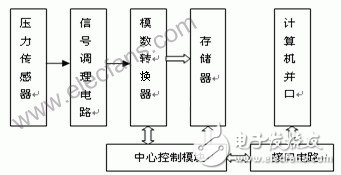
Figure 1 Working principle diagram of underwater shock wave recorder
3 CPLD applicationIn this design, the design is completed mainly using the CoolRuner CPLD chip developed by Xilinx. The XCR3256 device in this series is used in this design. It can realize 6000 gate digital logic circuits, embedded 256 macro cells, support 4 global clocks, low power consumption, fast ISP, delay predictable, etc. Features. We use XCR3256 chip to realize the main control module of underwater shock wave recorder. This main control module is used to control each peripheral device and coordinate the work of each peripheral device. The peripheral devices mainly include a power chipset, a static RAM memory, a crystal oscillator, an A/D converter, an LED, a parallel port, and the like. The crystal oscillator includes a 12 MHz crystal oscillator that generates a master clock and a 1 MHz crystal oscillator that generates a delay count clock. The block diagram of the main control module and each peripheral device is shown in Figure 2.
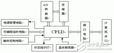
Figure 2 Block diagram of the main control module and peripheral devices of the underwater shock wave recorder
3.1 Flexibility and short development cycle The A/D converter in Figure 2 uses the AD7470. Its startup conversion input CONVST is divided by the main clock and the sampling frequency is programmable. The programmable delay circuit is realized by a four-way DIP switch to input different levels of CPLD input. By setting the CPLD digital logic to generate a 1MHz crystal oscillator count of the delayed count clock, input different level combinations to decode Different delay times are generated, and changing the level combination requires only the operation of the recorder's panel. CPLD devices with ISE development system can complete design input, compilation, verification and programming, design verification for complete simulation, worst case timing analysis and functional testing. Designers can reconfigure digital systems without a programmer, with the feature of "hardware hardware." 3.2 Low power consumption and high integration
The power chip in the power management circuit in Figure 2 mainly includes the MAX1658, MAX1659, and MAX1616. They all have a SHDN input. When the SHDN terminal is low, no matter how much voltage is input to the voltage input, the output voltage is 0V, and only when the SHDN terminal is high, when the input terminal is connected to a suitable voltage, the output terminal can generate the corresponding voltage value for the system to work normally. Since the device eventually works underwater, battery power is required, which requires the circuit to have low power consumption.
There are five states when the recorder works: low power consumption delay setting power-on state, low power consumption to be triggered state, data recording state, data hold state, read data state. The transition of the state is done under the control of the central control module. The system comes with a data-holding power supply, so the system is in data hold when not in use. After the main control module is powered on, the delay time is set by the four-way dip switch. After the delay time expires, other modules are automatically powered on, and are in the state to be triggered, ready to collect data. With the arrival of the trigger signal, the system state is switched to the data recording state. After the recording is completed, the system enters the low power data holding state and waits for the recovery. After the device is retrieved, the system changes to the read data state when the reading is completed. After the reading is completed, the system is in the data holding state again, waiting for the next recording. In this way, each time the system records, its corresponding state is cycled once. At different stages of the system operation, we can control the SHDN input of each power chip through the internal digital logic of the CPLD, so that the SHDN input of the chip that must be operated is set high, and the SHDN input of the chip that does not need to work is set low, thereby realizing Low power consumption.
Xilinx devices have an integrated range of 300 to 250,000 available gates, making it easy to integrate existing logic functions, whether they are composed of multiple discrete logic devices, multiple PLDs or FPGAs, or several custom The components of the device. In system design, increased integration means that the device scale is reduced, the number of components is reduced, and the reduction in the number of components inevitably reduces power consumption, especially the use of embedded array blocks (EABs), which can integrate memory into In the CPLD chip, it is especially beneficial to the design of the system on the chip, which reduces the cost of the system, the power consumption of the device, and can improve the performance and reliability of the system.
The use of CPLD devices for circuit design can significantly reduce printed board area, solder joints and connectors, reducing assembly and commissioning costs. A large number of discrete devices often cause failure due to poor soldering or poor contact during the electrical mounting of the printed circuit board, and such faults are often difficult to find, which brings great difficulties for debugging and maintenance. Therefore, after the CPLD device is used, the integration is improved, the number of components is reduced, and the number of printed boards is reduced, so that the combination of extensions is reduced, and the overall cost of the device is reduced, so that the reliability of the device is greatly improved.
Xilinx's CPLD development tool ISE supports a variety of input methods, which provides great convenience for design development. Therefore, the system is designed with ISE. It can easily design input, edit, and connect to the verification tool. Designers can use the standard EDA design input tool to build the logic design, and use the ISE compiler to compile the XCR3256 device. The design flow is shown in Figure 3.
Design input methods include schematic input, hardware description (HDL) language input, and waveform input. Each function block of the recorder circuit: generation of unidirectional bus buffer, generation of A/D clock signal, write signal and chip select signal, generation of address generator, read and write command and data transmission control, reading clock The debounce is implemented by the hardware description language (VHDL), and finally the function blocks are connected by the schematic input. The advantage of using language description is that the efficiency is higher, the result is easier to simulate, and the signal observation is more convenient.
Read information in the design file and generate programming files and simulation files and automatic error location, design rule checking and device partitioning. The compiler can also implement user-specified timing requirements, such as propagation delay (tPD), clock frequency. (f osc) and so on.
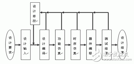
Figure 3 design flow
4.3 Design SimulationWhen the design is complete, the designer can verify whether the characteristics of the design circuit are consistent with the design purpose through simulation. Here, the timing function is used to test the logic function and the worst-case time relationship of the device. Through the simulation results, it is very straightforward to observe whether the results meet the design requirements.
4.4 Device ProgrammingAfter completing the design input and timing simulation operations, the final step is to program the XCR3256 device, which is configured by a computer through a Xilinx dedicated programming cable. The compiled configuration file is connected to the Xilinx dedicated programming cable via the computer parallel communication port, and then connected to the device. The programming interface allows the device to be configured using the programming software provided by the ISE development system. The advantage of this method is that it is convenient, quick and easy to modify. This is very beneficial for the debugging of the circuit. When debugging the circuit, it is often necessary to divide the circuit design to gradually debug. By changing the design, the device can be reprogrammed for easy circuit debugging.
5 ConclusionThe underwater shock wave recorder introduced in this paper is mainly used to test the strength of shock waves generated during underwater explosions. The design of CPLD devices is used to greatly improve the flexibility of system design, improve the reliability and integration of the system, and shorten the system. The cycle of product development can also reduce the design cost, save the PCB board area and wiring difficulty, improve the reliability of the equipment, and obtain satisfactory test results.
Outdoor Front Service LED Display
Front Service Outdoor Fixed Install LED Display Screen
1. High refresh rate: With NOVA STAR control system, no scanning line when photographed
2. High gray level: 256 RGB each ,display 16.7M colors ,vivid and perfect video effect
3.High resolution: The most apparent features of the new generation of LED display
4.Good color uniformity
5. High Brightness: 6000-8000 cd/m2 ,brightness automatically adjusted
6. High Quality: CE, RoHs, FCC, UL, IP65, ISO9001 passed + 96 Hours serious testing time
7. Long life span: over100,000hours, warranty from 2 years.
* Nova MSD 300 sending card and Nova mrv328 receiving card
* Cabinet size:960x960mm
* Kinglight/Nationstar LED Lamp, Refresh rate:1920-3840hz
* Ultra-Light designing, less than 30kg/pcs
* High brightness up to 6500cd/sq.m, even in the sunlight conditions can see clear, but low power consumption to save the electric power cost.
* High debugging brightness and no damage to gray scale, achieving the debugging technology for nice image.
* Passed the TÃœV,FCC,ROHS,CE cetification.
Outdoor Front Service LED Display,P3.91 Outdoor Led Screen,Led Stage Screen,Outdoor Led Screen Price
Guangzhou Chengwen Photoelectric Technology co.,ltd , https://www.cwstagelight.com