
Since the beginning of 2009, the Chinese research team has been making strenuous efforts. The first set of 90nm high-end lithography machines has been successfully exposed for the first time in the near future. Around 2022 is expected to complete the acceptance. This means that China's semiconductor materials and equipment (process technology) industry has taken another major step forward. Lithography machines are called "Pearl of Industry Crown" by people in the global industry. In fact, Chinese scientific research and engineering staff also have aspirations for the future, from the "industrial crown" to get this "pearl."
Domestic lithography machine reaches several nanometersThe SP lithography machine developed by the State Key Laboratory of Optoelectronics Microfabrication Optical Technology is the world's first lithography machine capable of 22nm single-shot imaging. Combined with multiple exposure technologies, it can be used to prepare information devices below 10nm. This is not only a major change in optical lithography in the world, but also will accelerate the promotion of Industry 4.0 and realize the good vision of manufacturing China 2025.
1, Shanghai Microelectronics Equipment Co., Ltd.
2. The 45th Institute of China National Science and Technology Corporation
3. Hefei Core Semiconductor Co., Ltd.
4, first Teng Optoelectronics Technology Co., Ltd.
5. Wuxi Shadowspeed Semiconductor Technology Co., Ltd.
In late September 2009, the advanced package lithography machine developed by Shanghai Microelectronics Equipment Co., Ltd. passed the factory process test of Jiangyin Changdian Advanced Packaging Co., Ltd. and formally signed a product sales contract. The lithography machine has the technical characteristics of “large field of view, large depth of focus, high stacking accuracy, edge exposure†and the like, and can meet the requirements of 8-inch and 12-inch wafer-level rewiring bump equal thickness adhesives in advanced packaging I arts. . Since the operation of the production line in November 2009, Jiangyin Changdian has successfully completed the multi-layer lithography production task of the first 8-inch "re-wiring and bumping" products using this equipment.
The successful development and use of the first domestic advanced package lithography machine marked that China has made gratifying breakthroughs in the innovation and development of key equipment for high-end packaging, and it is important for improving the independent innovation capability of China's integrated circuit manufacturing equipment, processes and materials technologies. significance.
On the afternoon of July 16, 2010, Shanghai Microelectronics Equipment Co., Ltd. ("SMEE") and Jiangyin Changjiang Advanced Packaging Co., Ltd. ("JCAP") jointly held the "First Advanced Packaging Machine" in Jiangyin, Jiangsu Province. The use of on-site briefing sessions and the signing ceremony of the SMEE and JCAP Strategic Cooperation Agreements. Ministry of Science and Technology, National Science and Technology Major Project “Very Large Scale Integrated Circuit Manufacturing Equipment and Complete Technology†Implementation Management Office and
The leaders of the overall expert group, the special advisory committee, the Shanghai Municipal Science and Technology Commission, Jiangyin Municipal Office and other units attended the Ding meeting. The Vice Minister of the Ministry of Science and Technology Cao Jianlin and other leaders made important speeches.
With the development of the integrated circuit industry, the integration degree of high-end chips has reached thousands to hundreds of millions of transistors, which promotes the development of chip packaging technology to higher density and higher performance, and makes bump-based packaging the mainstream technology for packaging. The performance of the lithography machine has also been greatly improved. The traditional proximity/contact lithography machine can no longer meet the development needs of high-performance, high-density, low-cost and other advanced packaging technologies. The advanced large-field-of-view, large-focus depth, and high-precision projection light Engraver has become a key equipment for advanced packaging production lines. In order to change the status of this type of advanced package lithography machine completely dependent on the import situation, Shanghai Microelectronics Equipment Co., Ltd. has successfully developed the advanced technology for flip-chip bump preparation under the support of major national science and technology projects and the Shanghai Science and Technology Commission and other departments. Packaging lithography machine. The model has independent intellectual property rights, and has achieved a series of innovative results in key technologies such as projection objectives, high-precision workpiece stage, alignment measurement, and software systems. It has applied for 74 national invention patents and has been authorized by the national invention patent. In 22 cases, 3 international invention patents were applied for.
In late September 2009, the advanced package lithography machine developed by Shanghai Microelectronics Equipment Co., Ltd. passed the factory process test of Jiangyin Changdian Advanced Packaging Co., Ltd. and formally signed a product sales contract. The lithography machine has the technical characteristics of “large field of view, large depth of focus, high stacking accuracy, edge exposure†and the like, and can meet the requirements for 8-inch and 12-inch wafer-level rewiring bump equal thickness adhesives in advanced packaging technology. Since the production line was put into operation in November 2009, Jiangyin Changjiang has successfully completed the first batch of 8-inch “re-wiring and bumping†products for multi-layer lithography production.
The successful development and use of the first domestic advanced package lithography machine marked that China has made gratifying breakthroughs in the innovation and development of key equipment for high-end packaging, and it is important for improving the independent innovation capability of China's integrated circuit manufacturing equipment, processes and materials technologies. significance.
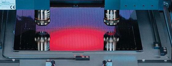
The minimum resolution, productivity, and yield of the lithography machine are all constantly evolving. The minimum resolution of the lithography machine is expressed by R=kλ/NA, where R represents the smallest resolvable size. For lithography, R is the smaller the better; k is the process constant; λ is the light source used by the lithography machine. Wavelength; NA represents the numerical aperture of the objective lens, which is related to the refractive index of the light propagation medium. The greater the refractive index, the greater the NA. The development of the lithography process technology level follows the above formula. In addition, the internal structure and working mode of the lithography machine are also developing, and the production efficiency and yield of the chip are continuously improved.
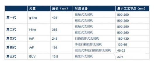
According to the improvement of the light source used, the lithography machine has experienced the development of the 5th generation product, and each time the light source improvement significantly enhances the minimum process node that the lithography machine can achieve. In addition, the innovation and development of new lithography technologies such as dual-tables and immersive lithography are also continuously improving the level of process technology of the lithography machine, as well as the efficiency and yield of production.
According to the light source used, the lithography machine has experienced the development of five generations of products
The first two generations of lithography machines used 436nm g-line and 365nm i-line produced by mercury lamps as lithography sources, which can meet the production of 0.8-0.35 micron process chips. The earliest lithography machines used contact lithography, ie masks were affixed to a silicon wafer for lithography, which was prone to contamination and had a short mask lifetime. Since then, the proximity lithography machine has improved the contact lithography machine, through the air cushion to create fine gaps between the mask and the silicon wafer. The mask and the silicon wafer are no longer in direct contact with each other. However, the accuracy of the imaging is not high due to the air cushion. .
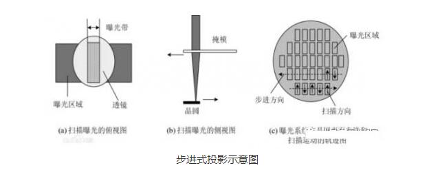
The third-generation lithography machine uses a 248-nm KrF (niobium fluoride) excimer laser as the light source to raise the minimum process node to the 350-180nm level. In the photolithography process, scanning projection lithography has also been adopted, ie, now lithography. General machine, the light source through the mask, adjusted and compensated by the optical lens, in a scanning manner to achieve exposure on the silicon.
Fourth-generation ArF lithography machine: The most representative lithography machine product. The light source of the fourth-generation lithography machine used a 193-nm ArF (argon fluoride) excimer laser to raise the minimum process to 65 nm in one stroke. The fourth-generation lithography machine is currently the most widely used lithography machine, and is also the most representative lithography machine. Because the lithography machine that can replace ArF to realize the lower process has been unable to develop successfully, the lithography machine manufacturer carries on a large number of technological innovations on the ArF lithography machine, in order to meet the smaller process and higher efficiency production demand.
Innovation 1: Achieve step-by-step scanning projection. In the previous scanning projection lithography machine, the silicon wafer was in a stationary state during photolithography, and the exposure of different areas of the silicon wafer was achieved through the movement of the mask. In 1986, ASML first introduced a stepper scanning photolithography machine, which realized the simultaneous movement of masks and wafers during the photolithography process, and used a reduced projection lens, reducing the ratio to 5:1, effectively improving the mask Using efficiency and exposure accuracy, the chip's process and production efficiency have been raised to a new level.
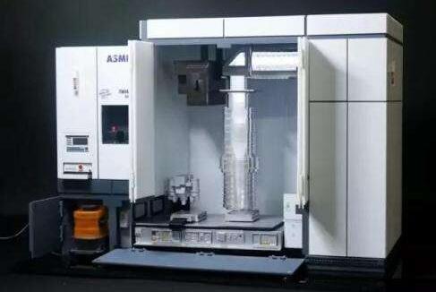
Innovation 2: Dual-table lithography machine. The silicon wafer must be measured and aligned before entering the photolithography process. In the past, the lithography machine had only one stage. Measurement, alignment, lithography, and other processes were performed on this stage. In 2001 ASML introduced the TWINSCAN system. The dual stage system allows the lithography machine to perform exposure without the need to change the initial speed and acceleration. At the same time, pre-alignment work before the exposure, so that the production efficiency of the lithography machine increased by about 35%.
Although from the results point of view, only one workbench is added, but the technical difficulty is not to be underestimated. The dual workbench system has extremely high requirements for the speed and precision of the exchange. If the exchange speed is slow, then the light will affect the light. Engraving machine work efficiency; If the channel changing accuracy is not enough, it may affect the normal development of subsequent scan lithography and other steps.
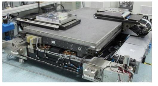
Dual table lithography machine prototype
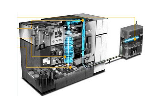
Innovation III: Immersion lithography system. At the 45nm process node, the ArF lithography machine also encountered the problem of insufficient resolution. At this time, the industry has proposed two roadmaps for the development of the next generation lithography machine. One is to develop a 157nmF2 excimer laser with a lower wavelength as a light source, and the other is immersion lithography proposed by Taiwan Semiconductor Manufacturing Co., Ltd. Lin Benjian in 2002. All the previous lithography machines were dry-type machines. Exposure and development were performed in a clean room using air as the medium. Since the NA in the minimum resolution formula is positively related to the refractive index, the minimum resolution will be improved if photolithography with water having a refractive index greater than 1 is used as the medium. This is the principle of the immersion lithography system.
ASML pioneered the introduction of immersion lithography machines to establish its market position. Lin Benjian proposed the concept of immersion lithography, ASML began cooperation with Taiwan Semiconductor Manufacturing Co., Ltd. to develop immersion lithography machine, and in 2007 successfully launched the first immersion lithography machine TWINSCANXT:1900i, the device uses a refractive index of 1.44 deionized water As a medium, the 45nm process technology was realized, and monopolized the market at one go. At that time, the other two major lithography giants Nikon, Canon's main 157nm light source dry lithography machine was abandoned by the market, not only lost a huge manpower and material resources, but also significantly behind the ASML product line, which is also Nikon, Canon by Sheng turn Decline, an important turning point for the ASML family.
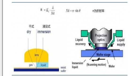
Immersion lithography principle
Through immersion lithography and double lithography processes, the fourth-generation ArF lithography machine can realize the production of chips up to 22nm process. However, under the impetus of Moore's Law, the semiconductor industry's demand for chip processes has been developed to 14nm, 10nm, Even 7nm, ArF lithography machines can no longer meet this demand, and the semiconductor industry hopes to ship to the fifth-generation EUV lithography machine.
The fifth-generation EUV lithography machine came out after a long time. The light sources used by the 1-4 generations of lithography machines are all deep ultraviolet light, and the fifth-generation EUV lithography machines use extreme ultraviolet light with a wavelength of 13.5 nm.
As early as the 1990s, the concept of the EUV lithography machine has been proposed. ASML also started the research and development of the EUV lithography machine in 1999. It was originally planned to introduce the product in 2004. However, it was not until 2010 that ASML developed the first prototype of the EUV. It only delivered downstream customers in 2016, more than ten years later than expected. Samsung, Taiwan Semiconductor Manufacturing Co., and Intel jointly acquired ASML to promote the development of EUV lithography machines.
There are two main reasons for the continuous delay of the EUV lithography machine's time-to-market schedule. First, the required power of the light source can not reach the operating power requirement of 250 watts. Second, the optical precision of the optical lens and mirror system is required. Extremely high, production is extremely difficult. These two major reasons make it difficult for ASML and its partners to support large research and development expenses. In 2012, Samsung's three major customers, Samsung, TSMC, and Intel jointly invested 5.265 billion euros in ASML to support the development of EUV lithography machines. Since then, ASML has acquired Cymer, the world's leading supplier of excimer lasers, and has invested EUR 1 billion in cash to acquire optical system supplier Carl Zeiss to accelerate the development of EUV light sources and optical systems. These two acquisitions have also been successful in the development of EUV lithography. important reason.
Lithography machine related articles:
Lithography machine structure composition and working principle
Domestic lithography machine level progress and prospect analysis
Why lithography machines in the Netherlands? Why lithography machines do not sell to China
Power Meter,Energy Meter, Best power meters,Cycling Power meters,Electrical power meter
NINGBO COWELL ELECTRONICS & TECHNOLOGY CO., LTD , https://www.cowellsocket.com