
Speech content
Hello, everyone, I'm Yannan Nan who is sharing today. I'm very honored to be able to communicate with you. What I share today is within my knowledge. I also want to ask people who I don’t understand to consult you.
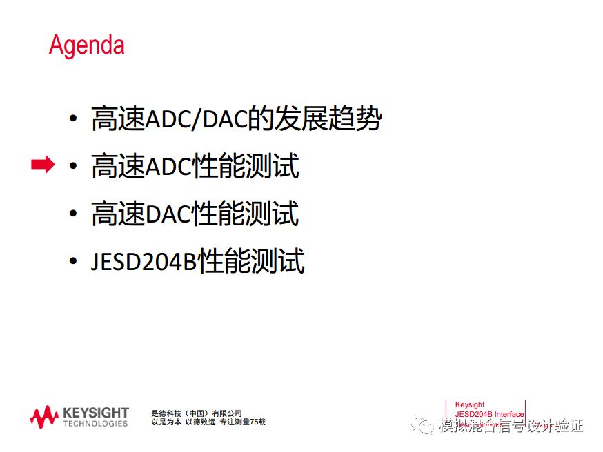
What I want to share with you today is the high speed ADC/DAC test method.
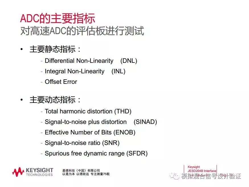
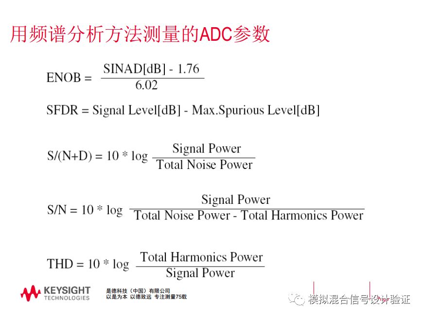
The main test indicators of ADC are divided into two categories: static indicators and dynamic indicators: static indicators, including INL, DNL; dynamic indicators, mainly based on SFDR, calculated on this basis ENOB (effective number of bits). Try to be concise.
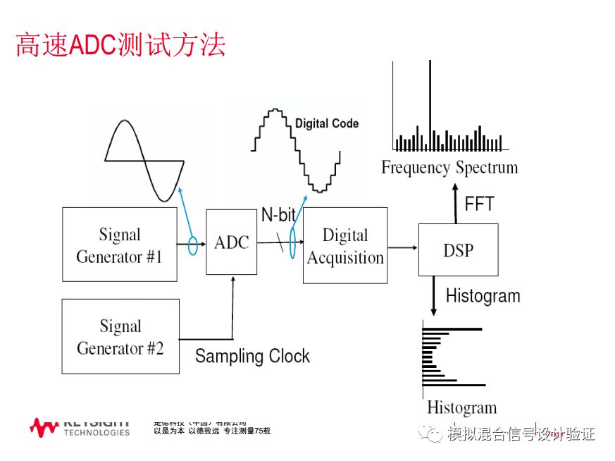
ADC test method, in simple terms, is the input and output, how to input? How to measure output? How to calculate? And converted to spec. The input is mainly two parts: data and clk. Do you know what ADC data and clk use for signals?
Audience A: ADC data refers to the input analog signal?
Teacher: Haha, yes, the signal generator; however, for ADCs, especially high-precision ADCs, the most critical is the choice of signal source, which requires a high-precision signal source, that is, the dynamic range of the signal source. This is one of the keys to being above the two precision bits of the ADC under test. The second is the synchronization of the source and the clk.
Next, let's look at the output. The ADC outputs a digital signal, which means that the output is sampling a digital signal. However, the dynamic parameter representation of the ADC is based on the method of spectrum analysis. That is to say, the output, sampled digital signal is transformed into the frequency domain by FFT, which is why we see the main test function of the ADC test program is the FFT function. I remember that our laboratory at that time measured at least 1024 points for ADCs with more than 10 bits.
Audience asked: Or go to the frequency domain, what precision is the accuracy of frequency?
Teacher: When you actually measure, sometimes you will find that there are few FFT points, and the test results will be good. I wonder if you have encountered this situation? Um, but this is actually an illusion. You want the full bit resolution of the 10-bit ADC output to be 1024. If you don't pick up 1024 points, you lose some of the data and don't really reflect the ADC's performance. Therefore, when we are testing, we cannot pursue occasional measurement of a good spec. Instead, we should focus on our own test methods and calculation methods, and whether it truly reflects the performance of the chip.
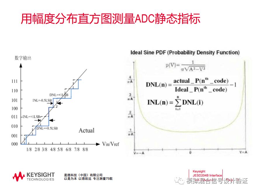
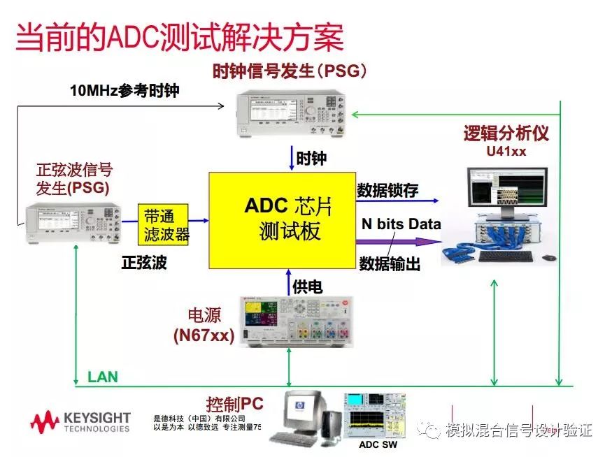
Just talked about dynamic indicators, static indicators are relatively easy to use, with high-end digital multimeter, not the kind of handheld, oh, is a professional programmable 6 and a half multimeter, the output is all down, using a simple formula can be calculated Out of INL and DNL, ​​this will not be wrong. The dynamic indicators SFDR and ENOB change due to changes in the number of FFT sampling points; but what the INL and DNL calculate is what there is and there is no question of digital conversion. The data frequency is the frequency of the largest input signal that the ADC can accept, say 100M; and the clock frequency is the sampling rate, say 1GS/s. When we were in school, we might feel that it would be good to send a paper for a good spec; but after work, it would be different. How is the chip in the end? I use a picture to summarize the most basic ADC, especially the basic method of testing parallel ADCs; we will talk about serial ADCs later.
Audience asked: 6-and-a-half meters to measure ADC? Should it be a DAC?
Teacher: It is ADC, digital output of ADC, can be measured with multimeter; DAC output is analog, continuous analog signal, can be seen directly with spectrum analyzer. Looking at this picture, in fact, all dynamic indicators are collected by logic analyzers. Just now, if INL and DNL think that a logic analyzer is complicated, it can be done with a multimeter. However, dynamic indicators must be acquired by logic analyzers. Oh, a little bit of leakage, between the signal source and the input of the ADC, to pick up the bandpass filter.
Times Q: The data captured by the logic analyzer was analyzed in MATLAB. Previously, adi had MATLAB routines.
Teacher: Times right! profession! So when people test the ADC, there is a necessary investment, which is to buy a few good quality bandpass filters with high roll-off coefficients. The bandpass filter is recommended for everyone to use that mini circuits. The last time I shared it was my girlfriend. When she was in our lab, our teacher gave her money to buy a lot of useful bandpass filters. Because the entire signal path, if the signal source quality is particularly good, particularly pure; ADC's ability is also very good, but the band-pass filter is not clean, the introduction of clutter, it is not worth the candle.
Hello everyone, the last picture I just made is probably the top one. This is a typical parallel port, is the parallel ADC, because if less is slow, we traditionally use the parallel output code, then I will talk about a serial port. Because if there is a big god of AD in the group, we know what the company is doing now. High-speed ADCs use serial ports. The parallel port is already a kind of technology that is earlier.
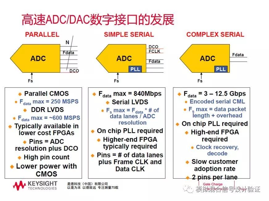
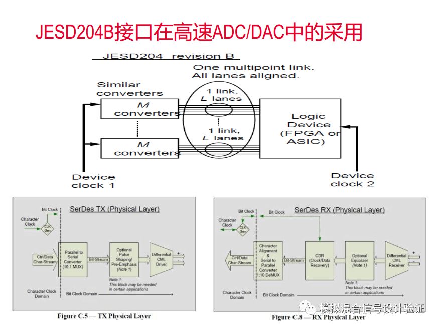
The serial port is like this. JESD204B is the interface specification of SerDes.
Audience Question: Taking 12-bit ad as an example, even if the input is at a stable level, the noise itself may cause a low 2-bit jitter. How can an accurate INL DNL be measured with a multimeter?
Teacher: We now see that the new 2GS/s ADCs/DACs made by ADI are all of this kind of interface. It's very advanced ~~ I converted ah, the 6 and a half multimeters can be measured after the decimal point. 6 Half in half. If 10bit ADC, input 1V, the minimum grid is 1/1024, that 4 and a half of the multimeter is enough.
The audience asked: lsb, not an absolute value.
Teacher: Oh~~ Where does the noise you say come from? power supply? AD itself, or input source? Haha, that waits for us to discuss this again.
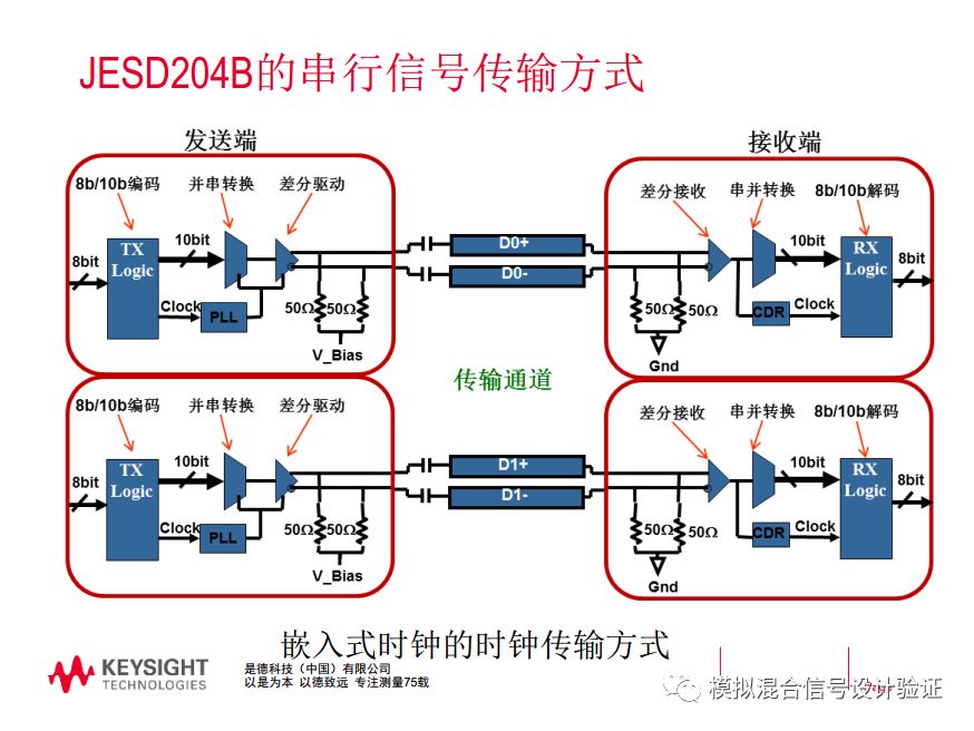
SerDes signal, we see the main difference between the parallel port and the parallel port on the receiver and the serial conversion, 8b/10b encoding, differential drive several modules. Although we design in these parts It takes a lot of energy, but at the time of testing, it becomes a black box. The main considerations are how to input the input signal, how to synchronize the clock, and how to collect the output signal.
I have a long story,
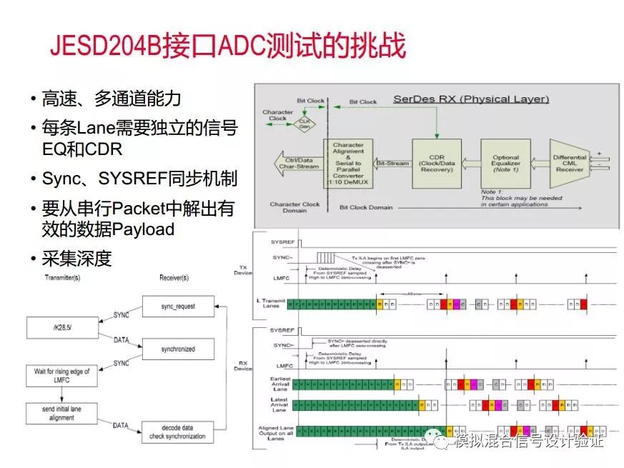
When it comes to Serdes testing, unlike the parallel port test, everyone saw this ppt ~ Fortunately, the test methods of Serdes are now also very mature, and the methods used by the major ADC design companies are roughly the same.
The audience asked: I feel that the clock PLL is a key link. Your keysight is just a logical analyzer option that supports the 204B interface. What the test engineer sees is the measured data.
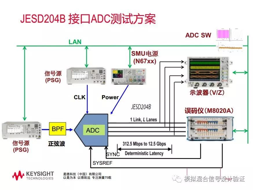
Teacher: You are right. Serdes compared with just the parallel test, the input signal has not changed, or use a high-purity signal source, high-purity, single-frequency point source, is the only requirement for the ADC input, once you have, there is no demand, the difference lies in the output part, In fact, it is the logic analyzer that supports the interface of 204B. It is guessed that the outcome is.
Audience asked: Can FPGAs with high-speed ports be used for the adc test of the 204b interface?
Teacher: As long as the interface is matched and the accuracy is sufficient, the ~~ sample rate is enough and the clock can be synchronized. Did you design your own FPGA board? How many bit ADCs are measured?
Audience asked: ADC digital output?
Teacher: The multimeter is a test DAC and gives input. There is no test ADC. FPGAs and logic analyzers are just like data acquisition boards.
Audience asked: DNL vs Noise, INL vs SFDR
Teacher: I remember when we used FPGAs in our lab, we didn't get clock synchronization.
Plug-In Connecting Terminals,Insulated Spade Terminals,Cable Connector Double Spade Terminals,Vinyl-Insulated Locking Spade Terminals
Taixing Longyi Terminals Co.,Ltd. , https://www.lycopperlugs.com