
Abstract: Based on FPGA, a high-speed digital down-conversion system is designed. The combination of parallel NCO and multi-phase filtering is used in the design to effectively reduce the data rate to suit the operating frequency of digital signal processing devices. In order to further improve the overall operating speed of the system, a large number of hard-core resources DSP48 in the FPGA are used in the design. Xilinx ISE14.4 analysis report shows that the circuit can work at speeds up to 360MHz. Finally, the simulation results in Matlab and ModelSim are given to verify the correctness of each module and the whole system.
Digital Down Conversion (DDC) is one of the key modules of software radio systems, which can convert high-frequency data stream signals into low-frequency data that is easy to process in real time by Digital Signal Processor (DSP) devices. Stream signal. In the digital down-conversion implementation, as the signal sampling rate continues to increase, the data rate will increase accordingly. However, as the data rate continues to increase in practical applications, the processing speed of data processing devices (such as FPGAs) will not meet the requirements. It does not work properly, which brings bottlenecks in digital signal processing. Based on multi-channel parallel NCO technology, this design studies how to use multi-channel parallel sampling data in FPGA to solve the problem that data processing devices can not provide high-rate matching signals, and gives the architecture of high-speed DDC implementation. And simulation results.
1 Basic principle of digital down conversionDigital down conversion is mainly composed of two parts: spectrum shifting and decimation, as shown in Figure 1. The spectrum shifting includes Numerically Controlled Oscillator (NCO), multiplier and low pass filter (LPF, Low Pass Filter); Includes decimation filter (LPF2) and D-times decimation, LPF2 is used to limit the spectrum of the signal to avoid aliasing after decimation.
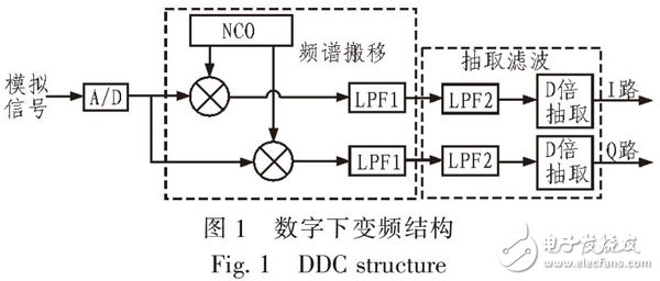
The analog signal is divided into two signals after A/D conversion, one signal is multiplied by the sinusoidal signal of the NCO output (in-phase component), and one is multiplied by the cosine signal of the NCO output (quadrature component), and then passed through a low-pass filter ( LPF1) filters out the high frequency components, and then the signal is decimate filtered to reduce the rate. The final two signals can be sent to the subsequent digital signal processor for further processing.
2 high speed DDC system designIn this paper, a high-speed DDC based on parallel NCO is designed, which can greatly reduce the processing speed of FPGA. The implementation is shown in Figure 2. The system is mainly composed of commutator, parallel NCO, multiplier module and two multiphase FIR. Filter composition. All circuits on the right side of the commutator operate at the clock frequency of Fs/4, the commutator will rate Fs, and the 16-bit data will become 4-channel Fs/4, 16-bit data. For applications where the input rate is high (for example, the rate exceeds 500M), the Xilinx hardware primitive IDDR is required for the input interface.
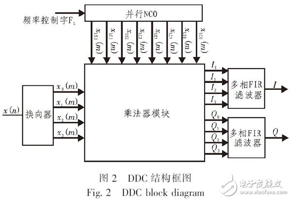
The commutator divides one high-rate data into four low-rate data outputs. The output frequency and initial phase of the parallel NCO are controlled by FL, respectively outputting 8 sine and cosine data, and the multiplier module realizes NCO output data and four low-rate data. Multiply, output four orthogonal components and four in-phase components, and then send the eight data into the low-pass filter for filtering, and finally output the in-phase component and the quadrature component separately.
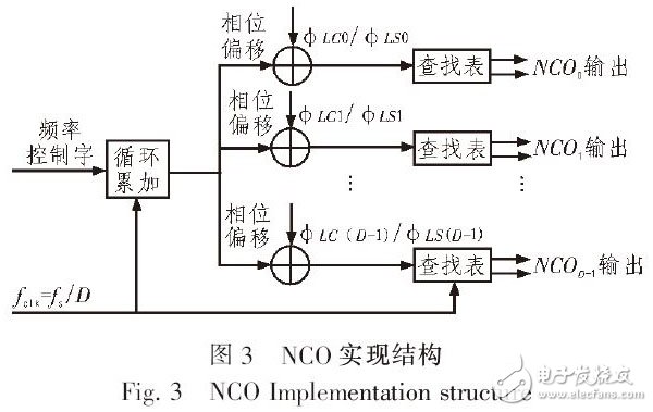
2.1 Parallel NCO design The NCO is a component for generating carriers cosωct and sinωct.
Assuming that the multiphase decomposition path of the NCO is D, we can write x(n) as follows:
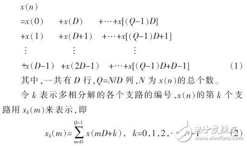
It can be seen from equations (1) and (2) that after polyphase decomposition, the data is changed from the original x(n) to D branches, and the sampling rate of x(n) is assumed to be fs, then the polyphase decomposition After that, the sampling rate of each branch is fs/D, that is, the data rate of each branch becomes fs/D, and the data arrival rate is slowed by D times compared with the original one (x).
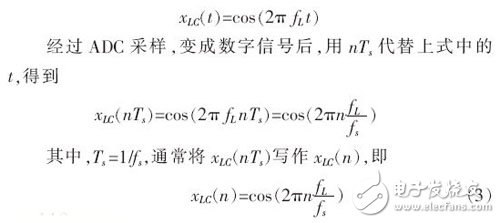
In Figure 1, the sampling rate of one way x(n) is fs, then the rate of the output carrier phase of the NCO must also be fs. Suppose the cosine signal of the NCO output to the upper branch is xLC(n), and the sine signal of the NCO output to the lower branch is xLS(n), assuming that the initial phases of xLC(n) and xLS(n) are both 0, the frequency Both are fL, we use xLC(n) as an example to illustrate. The analog signal before sampling is
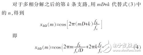
It can be seen from equation (4) that after the polyphase decomposition, although the sampling rate of each branch, that is, the rate at which data arrives, is reduced by D times, the frequency of the output of each branch NCO is still fL. We also need to further reduce the output local oscillator signal frequency of the NCO, because in general, the use of the NCO to generate the local oscillator signal requires the use of a main clock fclk. This main clock fclk must be a clock that the FPGA can run stably, and its frequency cannot be too high. Moreover, in practical applications, the frequency of the local oscillator signal output by the NCO cannot exceed the main clock fclk. Therefore, the required output frequency cannot be directly generated, but we can use the conversion relationship of the trigonometric function to generate indirectly. The NCO designed in this paper adopts the structure shown in FIG.
Precision Stainless Steel Band
Precision Stainless Steel Band,Decorative Stainless Steel Strips,Stainless Steel Belt Buckles,Stainless Steel Flat Trim Strips
ShenZhen Haofa Metal Precision Parts Technology Co., Ltd. , https://www.haofametals.com