
In this article, I will introduce an interesting clock chip feedback device. It may happen unexpectedly, or as an attempt to restore or test mode, but should generally be avoided as explained. In addition, understanding the Ouroboros clock may help explain some strange behaviors in complex timing applications. Before diving into the "Ouroboros" clock, let's take a look at the basic clock switching terminology and standard input clock switching configuration. Please click on " Read the original " to watch the full text!
Some basic clock switching terms
Clock chips typically support switching from one input clock to another based on certain qualifications (such as LOS ( Loss of Signal )) or OOF ( Out of Frequency ). The following are the most commonly used terms:
Free mode
Based on the output clock of an additional crystal or other resonator, or instead of an external reference clock. The frequency stability, drift and jitter characteristics of the output clock are determined by the crystal oscillator of the chip, independent of the input clock.
Hold mode
The output clock is based on historical frequency data for the selected input clock and is used when the input clock is lost and no valid spare is available. Usually historical data must be collected in some shortest time to be considered valid. The frequency accuracy is as good as the data collected.
Lock mode
The output clock frequency and phase are locked to the selected input clock, which is normal operation.
Standard input clock switching configuration
Consider the illustration of the two jitter attenuator clock IC cascades in the figure below. This may be used for additional jitter attenuation or for optimizing the planning and distribution of frequencies. To illustrate, these devices are depicted as a very simplified Si5345 block diagram. In the figure, IN0 and IN3 provide two input clocks to device # 1 .
In a typical application, one clock can be thought of as a " master " clock and the other as a " auxiliary " clock. The main clock may be recovered from network data, while the auxiliary clock is dependent on the local oscillator. If the primary clock fails or is disqualified by LOS or OOF , the clock chip switches to the secondary clock. This is usually intended to keep " downstream " equipment running. If the primary clock returns and is valid, the clock IC may be restored to it depending on the option selected .
The guess here is that as long as either of these two clocks are present, a valid lock mode clock is generated at OUT0 , thereby providing an input clock to downstream device # 2 . In fact, if both input clocks for device # 1 are lost, the device can enter the hold mode, as described above, even in free mode, and still produce a temporary reasonable output clock.
Clock configuration
In standard applications, the downstream clock is not fed back to the upstream clock input. Instead, they are typically scaled or jitter-attenuated versions of upstream independent stable or data derived clocks.
But what if we try the configuration shown in Figure 2 below? In this case, one of the outputs of downstream device # 2 is fed back to upstream device # 1 . This may be as a temporary backup clock.
Now as shown in Figure 3 below, what happens when we lose the main clock IN0 ? The auxiliary or alternate clock IN3 to device # 1 depends on the output of device # 2 . Note that this is just a locked version of Device # 1 output. We usually don't see this connection to a device, but occasionally come up with an application involving 2 devices.
This is the Ouroboros clock configuration. (Yes, it sounds like the lines of the big bang of life.) The name of ouroborus clock configuration is a mythical symbol that should be used for its feedback similar to a snake chasing (or biting) its tail. According to Wikipedia, the word comes from the Greek words "ourá" and "bóros" and is used to describe " swallowing or swallowing " . See the illustration in Figure 4 . It is an ancient cycle infinity symbol that is suitable for this application.

Gedanken
We consider a simple gedanken experiment consisting of a basic PLL . Then assume that it has been successfully placed in the Ouroboros configuration, as shown in Figure 5 below.
Now we can consider the possible consequences. If everything is ideal and there is no PFD (Phase Detector) error output, then the situation is at least slightly stable. However, even if the loop noise is ignored, it is likely that in the actual PLL , there is a fixed phase offset between the clocks presented between PFD ( + ) and PFD ( - ). In normal PLL operation, the VCO can be adjusted to lock the output clock frequency and phase to a separate input clock. In the Ouroboros configuration, the VCO cannot reduce the phase error.
Assume that the output clock is measured quickly in phase, under PFD ( + ) versus PFD ( - ). The loop will then attempt to track by tuning the VCO to a higher frequency. But the relative phase difference still exists. Therefore, the loop will continue to attempt to correct the measured phase error until the VCO is " fixed " at its highest frequency . Note that for generalization, the VCO can be tuned to a higher or lower frequency depending on the polarity of the phase difference . Most importantly, the PFD can see the phase difference that causes the runaway state.
experiment
So what happened under the real situation? Consider a project plan with the following attributes:
Nominal bandwidth: 100.000 Hz
Quick lock enable close
Exit from Holdover
OOF IN0 and IN1 :
Statement threshold 100 ppm
Assertion threshold 98 ppm
Now take such a plan, and apply them to two Si5345 evaluation board, the second portion shown above, except that instead of IN1 IN3 input clock as a secondary or backup.
Apply the signal generator to device # 1 IN0 and let both boards run until HOLD_HIST_VALID is true. What happens when I delete the 100 MHz input clock in IN0 ?
Initially only LOS [0] was reported by device # 1 . Otherwise everything is fine. However, the output clock frequency from Device # 2 starts to increase in frequency (usually it may rise or fall, but it is rising in my experiments).
Finally, the device # 2 is output as a standby clock input clock, far beyond the OOF apparatus # 1 standard. The settlement conditions are as follows:
Device # 1 enters hold mode
Device # 2 runs in lock mode.
Please note that in general, each device may be unreasonably unstable in the opposite state. Our experience is that most of the time there are some preferred states, but you will see alternatives from time to time, almost as if there is a chaotic element in the results.
In this case, ouroboros configuration doesn't really implement anything for us, except perhaps a little bit. However, please note that the output frequency is asserted at OOF [1] of device # 1 and device # 2 still depends on the device 1 HO clock for the entire time. This is only a potential problem for this unrealistic configuration. But there is another one that may be worse.
Ouroboros oscillation
This configuration can also produce a positive feedback system that can oscillate and cause strange behavior. In particular, this can happen if one of the devices can be taken to exit HO . For example, if the project plan OOF specification is tightened as follows, this phenomenon can be observed.
OOF IN0 and IN1 :
Statement threshold 000 ppm
Assertion threshold 9,375 ppm
Now these two devices will interact with each other and may never be resolved. Below is the frequency diagram of Device # 2 output clock data. You can see that the output frequency of Device # 2 slowly oscillates in the frequency range of 8 or 9 seconds.
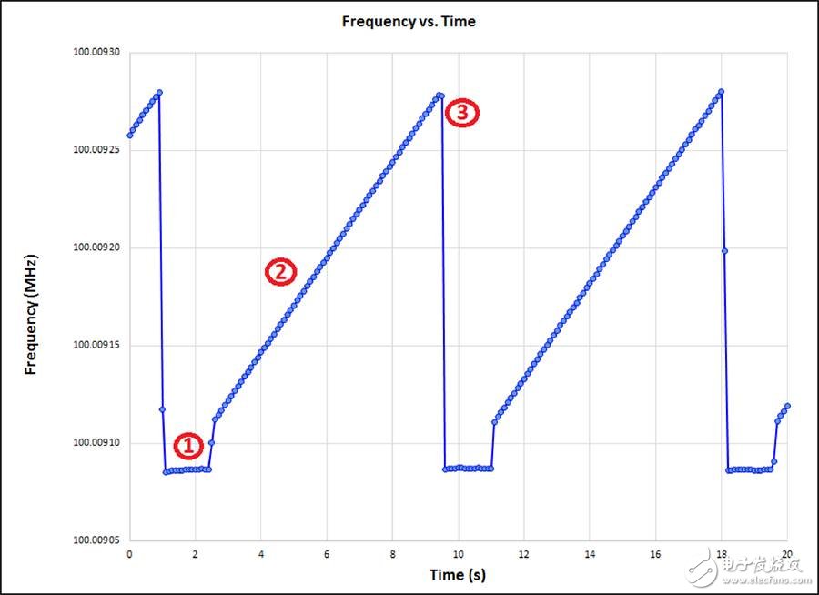
There are three functions on the status of device # 1 , because the output frequency of device # 2 is different:
1. Â Â Â Â Device # 1 is in hold or HO mode
2. Â Â Â Â Device # 1 exits from the HO ramp
3. Â Â Â Â Device # 1 is entering HO
During this time, device # 2 will not issue an alarm. This state can continue indefinitely. I started experimenting with this experiment on Friday afternoon and still running on Monday morning. The device can even exchange roles based on which state in the HO state! It is even worse for equipment to constantly enter and leave HO than to enter HO directly .
in conclusion
The bottom line is that ouroboros clock configuration either has no use other than delaying into HO , or can trigger oscillations that produce repeated roaming in the output clock. The downstream clock should generally remain downstream.
USB Flash Drives Compatible iPhone/iOS/Apple/iPad/Android & PC 128GB [3-in-1] Lightning OTG Jump Drive 3.0 USB Memory Stick
1. 3-in-1 OTG USB flash drive for PC, iPhone, Android, Type C
2. USB 3.0 + Android + IOS interface;
3. Capacity from 16~128GB;
4. Auto-run Function is optional;
5. Bootable Function;
6. Built-in Password Protection;
7. High speed Performance;
8. Data transfer rate for Read is from 12MB/s to 25MB/s, for Write is 4MB/s to 14MB/s in Dual-channel mode;
9. Data transfer rate for Read is from 8MB/s to 15MB/s, for Write is 2MB/s to 8MB/s in Single-channel mode;
(The rate of performance depends on the different operation system available and various flash adopted).
10. Operation Systems supported: No driver needed in Windows ME, Windows 2000, Windows XP, Mac 9.x or later, Linux Kernel 2.4 or later. Only Windows 98 and Windows 98SE need the enclosed driver;
11. 10 years data retention;
12. More than 1,000,000 times data encryption;
13. Built-in Password Protection is optional (default setting: NO password function);
14. Auto-run Function is optional (default setting: NO auto-run function);
15. Bootable Function is optional (default setting: NO bootable function);
16. ReadyBoost Function under Windows Vista system is optional (default setting: NO readyboost function).
Iphone Ios Usb Flash Disk,Portable 2 In 1 , 3 in 1 Usb Pendrive,Otg Usb Flash Drives,Portable Otg Usb Flash Disk
MICROBITS TECHNOLOGY LIMITED , https://www.hkmicrobits.com