
Abstract: On the basis of clarifying the principle and characteristics of single-tube flyback converter, it focuses on its important application in color TV. It points out the special requirements, technical difficulties and countermeasures of color TV power supply for flyback converter. The design example is introduced and the whole process of developing the TV power supply in the factory is given.
This article refers to the address: http://
Key words: color TV switching power supply; flyback converter; design
A Talkon Engineering Designof SMPS for Color TV
FENG Zhen-ye
Abstract:The special requests on flyback converter for TV sets, some techniques ticklers and countermeasures were discussed. A design example and the procedures for research and development of TV power supplies are also given.
Keywords:SMPS for color TV; Flyback converter; Design
1 Introduction
According to statistics, there are currently about 14 types of switching power supplies [1], and each topology has its proper application. As a power source for CRT TVs and monitors, the flyback converter has been regarded as its mainstream form. The reasons are as follows:
1) The flyback converter uses a transformer for coupling, which separates 'hot ground' from 'cold ground', which provides TV users with safety in use;
2) Compared with the forward converter with the same transformer, the secondary does not need to be connected to the high-voltage output choke and the expensive freewheeling diode, which saves space and reduces the cost;
3) The secondary multi-winding output, the main winding can easily achieve hundreds of volts DC output and has good input voltage and load change adjustment rate, as the secondary windings have a slightly lower adjustment rate than the load change of the main winding. At one point, the rest of the input voltage regulation rate can be equal to the main winding, which is not possible with the forward converter;
4) By carefully designing and adjusting the initial/secondary turns ratio of the transformer and the arrangement of the winding positions, it is possible to keep the flyback converter from maintaining the received image quality within the wide AC to AC range of 85 to 270V. Solved the world application problem of TV power supply;
5) Using only a single power tube as the switch is the most economical compared to other topological converters.
Of course, the flyback converter also has its limitations, which is limited by the performance of current power devices and core components. The single-tube output power can only reach about 200W, but it is enough for color TV applications, even if it contains heavy bass. The WOOFER function of the 34-inch large-screen color TV, its power output power is also about 145W. Therefore, from the perspective of performance and price ratio, most TV manufacturers are now willing to adopt such converters.
The author has been engaged in the research and development of color TV switching power supply for many years. Based on the past work experience, this paper attempts to talk about the basic principle and working mode of flyback converter from the perspective of color TV power supply application, the unique requirements of TV sets for flyback converters, and Engineering design method and debugging experience of single-tube flyback converter. I hope to help the industry and the majority of TV maintenance staff.
2 flyback converter principle and two working methods
The single-tube flyback converter circuit and its operating waveform are shown in Figure 1. When Q1 is driven by the input pulse and turned on, the primary current flowing through the Np winding rises linearly with a slope of VDC/Lp. At the end of the on time (ton), the primary current i1 has risen to the peak.
I1P= ![]() ×ton (1)
×ton (1)
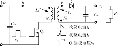
Figure 1 Basic circuit and waveform
At the same time, there is energy stored in the core.
E= ![]() (2)
(2)
When Q1 is turned off, the energy stored in the core is released to the secondary, because the current in the inductor cannot be abrupt, so at the beginning of the cutoff, the primary current is transferred to the secondary and the secondary current peak is
I2P=I1P ![]() (3)
(3)
This current will charge the output capacitor directly. After several cycles, the secondary DC voltage VO has been established. At this time, with Q1 being cut off, I2 will flow out from the NS.
I2=I2P- ![]() t (4)
t (4)
Equation (4) shows that i2 is linearly decreasing during the cutoff period, which reflects the core energy storage release. According to whether the magnetic core energy storage is completely released, the continuous and discontinuous working modes of the flyback converter can be derived, in fact, with the input of the mains voltage or the receiving load of the television (such as volume, brightness), the television Power supplies are likely to go through both ways of working.
1) Discontinuous operation mode If the mains voltage is low or the TV receiving load is too heavy, the secondary current i2 has dropped to zero before the next conduction of Q1, indicating that all core energy storage has been transferred to the load. After each turn of Q1, the corresponding primary current i1 and flux  rise from zero. This working state is called discontinuous mode, and its waveform is shown in Figure 2.
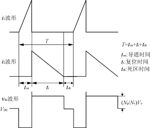
Figure 2 discontinuous waveform
At present, the power Pi input from the power supply VDC in one cycle T is
Pi= ![]() =
= ![]() (5)
(5)
Assume that the efficiency of the power supply is 80%, ie
Pi= ![]() =1.25
=1.25 ![]() =
= ![]() (6)
(6)
The output voltage NO obtained by equation (6) is
VO=VDCton ![]() (7)
(7)
Formula (7) Description:
(1) If the circuit of Figure 1 operates in a discontinuous mode, if the load RL is accidentally opened, the tube may be burnt out due to excessive output voltage VO, which occurs from time to time during commissioning;
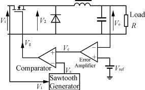
(2) Even if Figure 1 can work normally, its output voltage VO will change with the change of input voltage VDC and load RL, which is extremely unstable. In order to obtain a stable output voltage, a feedback regulator circuit is added as shown in Figure 3. It consists of an output voltage sampling divider, an EA error amplifier, and a variable width pulse generator controlled by a DC voltage. It can be seen from equation (7) that this feedback circuit must be able to reduce the ton when the VDC or RL rises, or raise the ton when the VDC or RL drops.
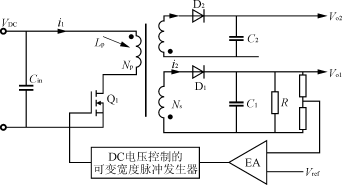
Figure 3 Converter with feedback regulator circuit
Calculation of the maximum voltage stress experienced by the power tube Q1:
During the Q1 cut-off period, because the secondary current i2 flows through the NS, the magnitude of the voltage generated on the NS is approximately the output voltage VO (ignoring the diode forward voltage drop and the lead loss), which reflects the induced electromotive force on the primary winding NP. VNP:
VNP= ![]() VO (8)
VO (8)
Therefore, the maximum voltage stress that the power tube Q1 is subjected to at the time of the cutoff is
VDSmax=VDCmax+VNP=VDCmax+ ![]() VO (9)
VO (9)
In practical use, the maximum voltage stress that Q1 is subjected to is not limited to VDSmax, but also the additional voltage spike caused by the leakage inductance of the transformer (estimated to be about 0.3 VDC), and when selecting a bipolar tube, it is required. Note that the sum of the two should be 30% smaller than the rated VCEO of the selected tube, so that there is sufficient safety margin.
2) Continuous operation mode If the mains voltage is increased or the receiving load is reduced, this causes the secondary current i2 to not fall to zero at the next turn-on of Q1, and the core still contains a part of the stored energy, which will be reflected to Primary, so that each time Q1 is turned on, the corresponding primary current i1 and magnetic flux φ do not rise from zero but from a constant value. This working state is called continuous mode, and its waveform is shown in Figure 4.
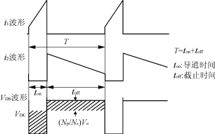
Figure 4 continuous mode waveform
It should be noted that according to the magnetic flux reset principle, there is a magnetic flux balance point φO in the continuous mode, and the magnetic flux increase amount Δφ1 at the time of conduction is equal to the magnetic flux reduction amount Δφ2 at the time of turn-off on the basis of φO, so
![]() VDCton=
VDCton= ![]() VOtoff
VOtoff
inferred
VO= ![]() VDC=
VDC= ![]() (10)
(10)
As can be seen from equation (10), if the circuit of FIG. 1 operates in a continuous mode, the output voltage VO depends only on the turns ratio NS/NP, the time ratio ton/toff, and the input DC voltage VDC, regardless of the load RL.
Similarly, the actual power supply should be added to the feedback circuit as shown in Figure 3. From equation (10), the function of this circuit should be to reduce ton when the input DC voltage VDC rises, or let ton decrease when the VDC decreases. Raise to keep the output voltage VO constant.
If we substitute equation (8) into equation (10), then
VDCton=VNPtoff (11)
Therefore, the formula (9) can be further simplified, that is, the maximum voltage stress that the power tube Q1 is subjected to can be turned into
VDSmax=VDCmax+ ![]() VO=VDCmax+
VO=VDCmax+ ![]() VDCmax=
VDCmax= ![]() (12)
(12)
Consider that the power tube is also subject to voltage spikes caused by the leakage inductance of the transformer (which is approximately 0.3 VDC max). Therefore the actual VDSmax' should be
VDSmax'=VDSmax+0.3VDCmax=1.3VDCmax+(NP/NS)VO (13)
3) Examples
There is a 29-inch TV whose maximum input mains voltage is AC 264V, transformer NP=32åŒ, NS=28åŒ, VO=140V, then VDSmax′=1.3× from equation (13) ![]() ×264V+160V=645V. In design, the VDS withstand voltage ≥VDSmax' should be selected for the MOSFET. The following describes the relationship between the input and output currents of the continuous mode and the load power.
×264V+160V=645V. In design, the VDS withstand voltage ≥VDSmax' should be selected for the MOSFET. The following describes the relationship between the input and output currents of the continuous mode and the load power.
Figure 5 shows the primary and secondary current waveforms in a continuous manner. Its output power is equal to the average of the output voltage multiplied by the secondary current pulse. ICSR is now defined as the midpoint value of the linear ramp portion of the secondary current pulse, so
PO=VOICSR ![]() =VOICSR(1-ton/T) (14)
=VOICSR(1-ton/T) (14)
ICSR= ![]() (15)
(15)
The midpoint value ICPR of the linear ramp portion of the primary current pulse in Figure 5 is derived from Pi = 1.25PO = VDCICPR ![]() Got
Got
ICPR= ![]() (16)
(16)
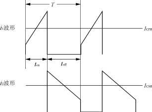
Figure 5 Primary and secondary current steps in continuous mode
It should be noted that the continuous mode appears just when the step of the primary current ramp occurs. It can be seen from Fig. 5 that when the ICPR rises to be equal to half of the slope amplitude ΔI1P, the current step begins to appear, and the ICPR at this time is in the continuous mode. The smallest, combined (16) has
ICPRmin= ![]() ΔI1P=
ΔI1P= ![]()
or
ΔI1P= ![]() (17)
(17)
The tonmax of the above formula can be found by the formula (11) at a given minimum VDCmin. Also because ΔI1P=(VDCmin)ton/LP
LP= ![]() =
= ![]() (18)
(18)
Using equations (10) to (18), the values ​​of the relevant parameters of the flyback converter operating in the continuous mode can be calculated. It should be pointed out that designing the flyback converter in two ways will yield very different results. For example, the literature [1] used a discontinuous and continuous operation to design a DC/DC flyback converter operating at 50 kHz. Assuming that the input DC voltage is 38V, the output is 5V, and the output power is 50W, the primary inductance is The LP and the primary and secondary currents will produce very different results as shown in Table 1 below.
Table 1 Comparison of Flyback Converter Designs in Different Modes of Operation
| Calculation results | Working in a discontinuous way | Working in a continuous manner |
|---|---|---|
| Primary inductance LP/μH | 52 | 791 |
| Primary peak current / A | 6.9 | 2.77 |
| Secondary peak current /A | 62.0 | 24.6 |
| Ton/μs | 9.49 | 11.86 |
| Toff/μs | 6.5 | 8.13 |
4) Comparison of the two working methods
It can be seen from Table 1 that the two modes of operation of the flyback converter have very different operating characteristics. The advantage of the discontinuous approach is that it reacts quickly to sudden changes in load current or input voltage, which results in a small instantaneous change in the corresponding output voltage. However, the disadvantage is that the secondary peak current is 2 to 3 times the continuous mode (relative to the same output current average). Therefore, at the beginning of the switching transistor cut-off, the discontinuous mode will have a large transient output voltage spike, which will require a larger LC filter to eliminate it. An excessive secondary peak current formed at the beginning of the switching tube cutoff simultaneously causes an RFI problem. Even for medium power outputs, due to the large di/dt value entering the output bus inductance, it generates very severe noise spikes on the output ground. Since the discontinuous secondary current rms value is nearly twice as high as the continuous mode, this requires a larger secondary wire diameter and an output filter capacitor with a larger ripple current rating. At the same time, the secondary output rectifier diode must also withstand high temperature rises. In addition, the primary peak current is also twice as large as the continuous mode. As shown in FIG. 2, in the case where the current average value is the same, the peak value of the discontinuous mode triangular current waveform is obviously higher than the peak value of the continuous mode trapezoidal waveform. As a result, it is required that the switching tube of the discontinuous mode has a higher current rating, resulting in an increase in cost. Similarly, higher primary currents can also cause severe radio frequency interference (RFI) problems.
Although the discontinuous approach has so many disadvantages, most power supplies are designed in this way because: First, the discontinuous approach requires a small primary inductance, which makes it possible to output load current or input voltage. The mutation responds quickly, so that the corresponding instantaneous output voltage ΔVO does not change much (less than 0.2V). Second, although the continuous mode has lower initial and secondary currents, this is an advantage, but it requires a large LP. And make its transfer function have a right half-phase plane zero, which is easy to cause instability of the closed-loop circuit. Therefore, as a general-purpose switching power supply, fewer people choose a continuous mode. However, as the color TV switching power supply has a large range of input voltage, it is often designed in a discontinuous manner at the low end of the voltage. However, at the middle and high end of the voltage, the circuit still inevitably enters a continuous mode. At this time, the converter changes suddenly to the load current. (such as image brightness, sudden change in volume, etc.) The response is slow, and the instantaneous change VO of VO is increased (about 0.2 to 0.5V), which directly affects the change of the output voltage of each winding of the output stage transformer. Thanks to the amount of CRT current and the high voltage of the anode. It is increased (decreased) at the same time. When the beam current is hit on the screen, the change of the anode high voltage will be weakened. If the adjustment is appropriate, most of the influence on the image jitter caused by ΔVO can be eliminated. Of course, we should pay attention to this time. The error amplifier bandwidth in the feedback loop is narrowed to allow for stable operation of such converters.
5) PWM control method
In practical applications, the single-tube flyback converter has two types: self-excited and excited. Self-excited circuits are simple, but have poor regulation performance and are only suitable for low power applications. In the early 14- to 21-inch small-screen color TV sets, there was no shortage of such inverters composed of fully discrete components. However, its current type has been widely used. It uses an external control IC with a driver stage to control the switching tube operation, mainly using pulse width modulation (PWM). However, there are various ways to implement PWM, among which are:
(1) directly controlled by duty cycle
As shown in Figure 6. Comparing the control voltage VC with a fixed frequency sawtooth voltage results in a variable width pulse that controls the on-time of the switching transistor.

(a) Schematic
(b) Comparator input
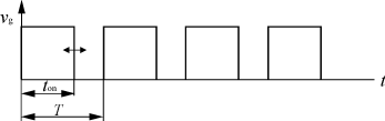
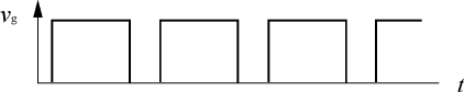
(c) vg
Figure 6 Direct duty cycle control
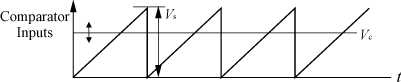
(2) Voltage feedforward control
It is very similar to duty cycle control, but the difference is that the current sawtooth voltage amplitude VS is proportional to the input voltage Vi, as shown in Figure 7.
(a) Schematic
(b) Comparator input
(c) vg
Figure 7 Buck voltage feedforward control
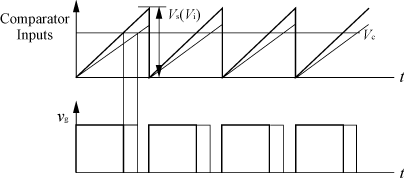
(3) Current control
This is a widely used technology in SMPS. The control voltage VC is no longer compared to an independently generated sawtooth voltage, but instead VC is compared to a voltage proportional to the primary current to form a second internal control loop. As shown in Figure 8.
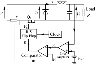
(a) Schematic
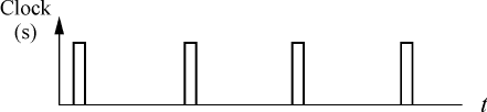
(b) Clock pulse

(c) Comparator input
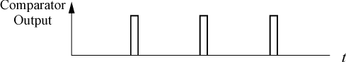
(d) Comparator output
(e) vg
Figure 8 Buck current mode control
(4) Quasi-resonant technology
Current control, but toff also slightly delays to make the switch conduct under the lowest electrical stress. This is called current-mode PWM plus quasi-resonance technology. This is currently the most commonly used.
Signal
Response time refers to the response speed of the Liquid Crystal Display to the input signal, that is, the response time of the liquid crystal from dark to bright or from bright to dark (the time for the brightness from 10%-->90% or 90%-->10%) , Usually in milliseconds (ms). To make this clear, we have to start with the human eye's perception of dynamic images. There is a phenomenon of "visual residue" in the human eye, and the high-speed motion picture will form a short-term impression in the human brain. Animations, movies, etc. to the latest games have applied the principle of visual residue, allowing a series of gradual images to be displayed in rapid succession in front of people's eyes to form dynamic images. The acceptable display speed of the picture is generally 24 frames per second, which is the origin of the movie playback speed of 24 frames per second. If the display speed is lower than this standard, people will obviously feel the picture pause and discomfort. Calculated according to this index, the display time of each picture needs to be less than 40ms. In this way, for the liquid crystal display, the response time of 40ms becomes a hurdle, and the display above 40ms will have obvious picture flicker, which makes people feel dizzy. If you want the image screen to reach the level of non-flicker, it is best to achieve a speed of 60 frames per second.
I used a very simple formula to calculate the number of frames per second under the corresponding response time as follows:
Response time 30ms=1/0.030=approximately 33 frames per second
Response time 25ms=1/0.025=approximately 40 frames per second
Response time 16ms=1/0.016=approximately 63 frames per second
Response time 12ms=1/0.012=approximately 83 frames of pictures displayed per second
Response time 8ms=1/0.008=approximately 125 frames per second
Response time 4ms=1/0.004=approximately 250 frames per second
Response time 3ms=1/0.003=approximately display 333 frames per second
Response time 2ms=1/0.002=approximately 500 frames per second
Response time 1ms=1/0.001=approximately 1000 frames per second
Tip: Through the above content, we understand the relationship between response time and the number of frames. From this, the response time is as short as possible. At that time, when the LCD market first started, the lowest acceptable range of response time was 35ms, mainly products represented by EIZO. Later, BenQ's FP series came out to 25ms. From 33 to 40 frames, it was basically undetectable, and it was really quality. The change is 16ms, displaying 63 frames per second to meet the requirements of movies and general games, so 16ms is not obsolete. With the improvement of panel technology, BenQ and ViewSonic started a speed battle. ViewSonic started from 8ms to 4ms. Released to 1ms, it can be said that 1ms is the final controversy of LCD speed. For game enthusiasts, 1ms faster means that CS's marksmanship will be more accurate, at least psychologically, such customers should recommend the VX series of monitors. But everyone should pay attention to the grayscale response when selling. The text difference in full-color response may sometimes mean the same thing as gray-scale 8ms and full-color 5ms. It is the same as when we sold CRTs before, we said that the dot pitch is .28, LG just I have to say that he is .21, but the horizontal dot pitch is ignored. In fact, the two are talking about the same thing. LG has come up with a sharpness of 1600:1. This is also a conceptual hype. Everyone uses the basic screen. There are only a few companies on the list, and how can only the LG family achieve 1600:1, and everyone stays at the level of 450:1? When it comes to consumers, the meaning of sharpness and contrast is obvious, just like AMD's PR value, which has no real meaning.
Active Matrix Lcd,Active Matrix Tft Color Lcd,Tft Lcd Color Monitor,Tft Lcd Monitor
ESEN Optoelectronics Technology Co., Ltd, , https://www.esenlcd.com