
In the second half of the 20th century, with the rapid development of integrated circuits and computer technology, the digital system has also developed rapidly. Its implementation method has gone through the process of discrete components, SSI, MSI, LSI, VLSI, and UVLSI. At the same time, in order to improve the reliability and versatility of the system, microprocessors and application-specific integrated circuits (ASICs) have gradually replaced general-purpose full-hardware LSI circuits. In both of these, ASICs are small, lightweight, and consume low power. , speed, low cost, and good confidentiality come to the fore. In general, the fabrication of ASICs can be broadly divided into masking methods and field programmable methods. At present, a large number of programmable logic devices (PLDs), especially field programmable logic devices (FPLDs), are widely used in the manufacture of ASICs. In the development of programmable integrated circuits, electronic design automation (EDA) technology has emerged. The emergence of EDA technology has not only brought about a revolutionary change in the design of electronic systems. From a certain point of view, it has also become an inevitable development.
1 The basic characteristics and development of EDA technology1.1 Basic Concepts of EDA Technology
EDA (Electronics Design AutomaTIon) is electronic design automation technology. It is a computer-based basic work platform that was developed using computer graphics, topological logic, computational math, and artificial intelligence. A complete set of software tools is an integrated technology that helps electronic design engineers engage in the design of electronic component products and systems.
1.2 Development and Development Trend of EDA Technology
The development of EDA technology has gone through a shallow to deep process. In the 1970s, with the development and application of small and medium sized ICs, the traditional methods of manual graphic design for printed circuit boards and integrated circuits could not meet the requirements of design accuracy and efficiency. Therefore, engineers began to implement two-dimensional graphic computer. Assist design to unburden complex, mechanical layout work, which resulted in the first generation of EDA tools.
In the 1980s, in order to meet the needs of electronic products in terms of scale and production, the second generation of EDA technology with computer simulation and automatic routing as the core technology was introduced. Its characteristics are based on software tools. Through these softwares, all aspects of product development such as design, analysis, production, and testing are completed.
After the 1990s, EDA technology continued to develop, and third-generation EDA technology featuring high-level language descriptions, system-level simulations, and integrated technologies emerged. Their appearance has greatly improved the efficiency of system design, so that the majority of electronic designers began to realize the dream of "concept-driven engineering." Designers get rid of a large number of assisted design work, and focus on creative solutions and conceptual concepts, which greatly improve the design efficiency and shorten the product development cycle.
Thus, EDA technology can be seen as an advanced stage of electronic CAD. The advent of EDA tools brought revolutionary changes to the design of electronic systems. With the introduction of Intel's PenTIum processor, companies such as Xilinx have introduced hundreds of thousands of gate-size FPGAs, as well as large-scale chipsets and high-speed, high-density printed circuit board applications, EDA technology in simulation, timing analysis, integrated circuits Automated testing, high-speed printed circuit board design, and expansion of the operating platform are all facing new and enormous challenges. These problems are actually the trend of the future development of the new generation of EDA technology.
1.3 Basic Features and Basic Tools of EDA Technology
In general, the basic features of modern EDA technology are high-level language descriptions with system-level simulation and synthesis capabilities. It mainly adopts concurrent engineering and "top-down" design methods, so that developers must consider many aspects of the product generation cycle from the very beginning, including quality, cost, development time, and user needs. Then start from the system design, divide the functional block diagram and structure design at the top layer, perform simulation and error correction at the block diagram level, and describe the high-level system behavior with hardware description languages ​​such as VHDL, Verilog-HDL, and ABEL. One level of verification, and finally use the logic synthesis optimization tool to generate a specific gate-level logic circuit netlist, the corresponding physical implementation level can be printed circuit boards or application-specific integrated circuits. In recent years, the gradual standardization of design data formats, such as hardware description languages, and different design styles and application requirements have led to the integration of unique EDA tools on the same workstation, thus making the EDA framework increasingly standardized.
The development of EDA tools has gone through two major stages: physical tools and logical tools. Now EDA and system design tools are gradually being understood as a whole concept: electronic system design automation. The physical tools are used to complete the actual physical problems in the design, such as chip layout, PCB layout, etc. The logic tools are based on the concepts of netlist, Boolean logic, transmission timing, etc. They are first designed by schematic editor or hardware description language. Input, and then use the EDA system to complete the synthesis, simulation, optimization and other processes, and finally generate a netlist or a structured description of VHDL, Verilog-HDL that the physical tool can accept. Common EDA tools now include editors, simulators, check/analysis tools, optimization/synthesis tools, and more.
At present, PLD has become the main means of modern digital system design. The traditional programming technique is to insert the PLD device on the programmer for programming, and the “In-System Programmable†(ISP) logic device is developed, and the superiority of the programmable device is brought to the extreme. It allows the user to "edit in the system" and modify the logic, providing the user with the ability to reconfigure the system without modifying the hardware design of the system and the ability to upgrade the hardware, making the hardware modifications as convenient as the software modifications. Reliability therefore increases. ISP technology is a technology that directly programs PLD devices in a user-designed target system or on a circuit board. It breaks the convention that PLD must be programmed after assembly, and can be programmed after assembly, and can be programmed repeatedly after becoming a product. Thus creating a new page of digital electronic system design technology.
Next, the author takes the design of a simple four-bit twist ring counter (ie, four-bit circular lantern) based on Xilinx-based CPLD devices XC95108-7PC84C and FoundaTIon 2.1 software platform as an example to discuss the EDA technology in the ISP digital logic system. The specific application.
2 Application of EDA technology in a simple digital system design2.1 Design requirements
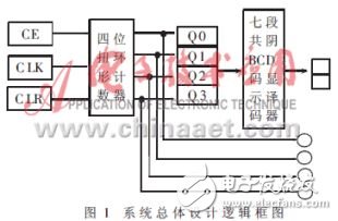
This system requires the design of a four-bit twisted ring counter. The rising edge of the clock triggers the reset (ie, clearing) and clock enable control. The result requires display through four in-line LEDs (constitutes a simple The lantern pattern is circulated. At the same time, its output reading (hexadecimal) also requires display through the nixie tube.
2.2 Design Analysis
According to the design requirements, the system can complete the counting part through four D-flip-flops with clock enable and asynchronous clear-end triggering, and the clock synchronization, if the initial value of the four-bit output is “0000â€, go through 8 The output of the clock pulse excitations are: "0001" (1), "0011" (3), "0111" (7), "1111" (F), "1110" (E), "1100" (C) , "1000" (8), "0000" (0). The output of these moments, on the one hand, will be sent to the LED for display; on the other hand, it will be sent to the seven legs of the digital tube, and the reading will be displayed through a seven-segment common-tone BCD code display decoder. The overall logic diagram is shown in Figure 1.
2.3 Concrete realization
After the overall analysis of the "top-level" design, you can use EDA tools and ISP technology to "down" the specific module design.
2.3.1 Logical Input
2.3.1.1 Counter section
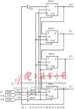
One of the important features of the EDA tool is support for multiple input methods, such as schematic input method, state machine input method, HDL high-level language input method, and so on. The FoundaTIon 2.1 software platform supports all three input methods. The design of this part is based on the schematic input method as an example. The four bit torsion ring counter schematic diagram is shown as in Fig. 2.
2.3.1.2 Digital Tube Display Section
In essence, a 4- to 7-line BCD code display decoder is designed. This part is designed to use IEEE common hardware description language VHDL to design, complete the compilation and synthesis will generate the corresponding macro module, the design code is as follows:
Library IEEE;
Use IEEE.std_logic_1164.all;
Entity HEX2LED is
Port (
HEX: in STD_LOGIC_VECTOR (3 downto 0);
LED: out STD_LOGIC_VECTOR (6 downto 0)
);
End HEX2LED;
Architecture HEX2LED_arch of HEX2LED is
Begin
With HEX SELect
LED<=“1111001†when “0001â€, -1
"0100100" when "0010", --2
"0110000" when "0011", --3
"0011001" when "0100", --4
"0010010" when "0101", --5
"0000010" when "0110", --6
"1111000" when "0111", --7
"0000000" when "1000", --8
"0010000" when "1001", -9
"0001000" when "1010",--A
"0000011" when "1011",--b
"1000110" when "1100",--C
"0100001" when "1101",--d
"0000110" when "1110",--E
"0001110" when "1111",--F
"1000000" when others;--0
End HEX2LED_arch;
2.3.1.3 LED display section
The display of the luminous tube only needs to directly connect the output leads of Q0-Q3 with four parallel arranged light emitting diode pins.
At this point, the design work of each part is basically completed. We only need to connect each part strictly according to the wiring rules. After defining the corresponding I/O pins and signal lines, we can implement the logic and synthesis.
2.3.2 Logic Implementation and Synthesis
EDA provides good logic synthesis and optimization functions. It can automatically convert logic level circuit diagrams designed by designers to gate-level circuits, and generate corresponding netlist files, timing analysis files, and various reports. If there are no errors in the design, Finally you can generate a JED file that can be downloaded programmatically.
2.3.3 System Simulation
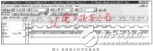
In general, before the formal download, the designer must also perform some verification work on the designed circuit, and these tasks can be completed through EDA's functional simulation and timing simulation tools. When the system has set CLK, CE and CLR signals, the functional simulation diagram and timing simulation diagram of the output QO-Q3 are shown in Figure 3 and Figure 4, respectively. It can be seen from Fig. 4 that the delay of each signal of this design is about 2ns, which basically meets the design index requirements.

2.3.4 Programming Download
When the designer determines that the design work has been largely successful, hardware verification can be performed by downloading the data stream via the programming cable. After the verification is passed, the overall design work is completed successfully.
Through the design flow of this example, it can be known that EDA technology and its tools are playing an increasingly important role in digital circuit systems (including analog circuit systems), and its depth and breadth of applications are being extended to a deeper level.
At present, the development of modern integrated circuit technology has enabled the rapid increase in the number of equivalent gates of large-capacity programmable logic devices represented by field programmable gate arrays. The scale of the equivalent number of gates is almost equal to that of standard gate arrays, achieving the level of system integration. Especially after entering the 1990s, with the rise of field programmable logic devices such as CPLDs and FPGAs, the popularity of hardware description languages ​​such as VHDL and Verilog, and their portability, and the continuous improvement of ASIC technology, EDA Technology plays an increasingly important role in modern digital systems and microelectronics applications. In a general sense, the design of modern electronic systems has already been separated from the help of EDA technology.
This 12 port Usb charger has strong compatibility and can support iPad, iPhone, Samsung Huawei, tablet and other devices. At the same time, this type of 12 port mobile phone charger with built-in smart IC chip can automatically provide the best current for your device, which can provide up to 2.4A, increasing the charging speed by 30%.

12 Port Usb Charger,Ipad High Charger,12Port Mobile Phone Chargers,12Port Usb High Power Charger
shenzhen ns-idae technology co.,ltd , https://www.best-charger.com