
Low-profile piezoelectric speakers provide superior sound for portable electronic devices, but require voltage swings across the speaker components to be greater than 8Vp-p. However, most portable devices have only one low-voltage power supply, and conventional battery-powered amplifiers do not provide a large enough voltage swing to drive the piezoelectric speaker. One way to solve this problem is to use IC1 in Figure 1. You can configure IC1 to drive a piezoelectric speaker with a voltage swing of up to 12Vp-p and power from a 3V supply. The IC1 model is the MAX4410, which includes a stereo headphone driver and an inverting charge pump that draws a negative 3V supply from a positive 3V supply.
Therefore, an internal ±V supply to the driver amplifier provides a 6Vp-p swing for each output of IC1. By configuring IC1 as a BTL (bridge) driver, the maximum voltage swing across the load can be doubled to 12Vp-p. In the BTL architecture, the right channel of IC1 acts as the main amplifier, which determines the gain of IC1, drives one end of the speaker, and provides a signal to the left channel. If IC1 is configured as a follower with a gain of 1, the left channel inverts the output of the right channel and drives the other end of the speaker. To ensure low distortion and good matching, you should use a precision resistor to adjust the gain of the left channel.
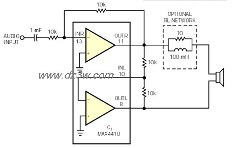
Figure 1. This bridge-type load configuration doubles the voltage swing of the amplifier. We tested the circuit with Panasonic's WM-R57A piezoelectric speaker and plotted THD+N (total harmonic distortion + Noise) curve (Figures 2 and 3). It is to be noted that in Figures 2 and 3, the total harmonic distortion and noise increase with increasing frequency. Because a piezoelectric speaker is almost a capacitor for an amplifier, the impedance of the speaker decreases as the frequency increases, with the result that a larger current is drawn from the amplifier.
IC1 does not vary with this speaker, but speakers with different characteristics may cause instability (Figure 4). In that case, you can add a simple resistor/inductor network in series with the speaker to isolate the speaker's capacitance from the amplifier (in the dotted line in Figure 1). This network maintains a minimum high frequency load of approximately 10 Ω at the output of the IC to maintain circuit stability.
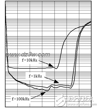
Figure 2 The THD+N vs. output voltage curve for the Figure 1 circuit is plotted against the test of the circuit.
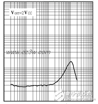
Figure 3 The THD+N vs. frequency curve for the Figure 1 circuit is based on tests for this circuit.
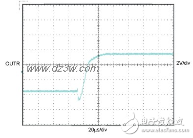
Figure 4 Figure 1 shows the step response of the OUTR output of a WM-R57A piezoelectric speaker IC1, indicating that IC1 does not change with the speaker.
The 3.3-B input is converted to a 12V (15V) isolated output supply using an H-bridge transformer driver (MAX256) and LDO (MAX1659) (Figure 1). This versatile power solution can be used for isolated power applications in a variety of applications, but primarily for industrial sensors, industrial automation, process control, and medical electronics.
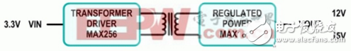
Figure 1. Block diagram of the Riverside subsystem design
Laboratory measurementTest the designed 12V and 15V output cases, and adjust the R2 and R3 resistance values ​​to obtain other output voltages.
When set to 12V output, the circuit can provide a maximum load current of 165mA. When set to 15V, a load current of 60mA can be supplied.
In order to improve the load driving capability, the user can increase the voltage of the input power supply or appropriately increase the transformer turns ratio. For more information, please refer to the MAX256 data sheet. Power efficiency is noted in Figures 2 and 3.
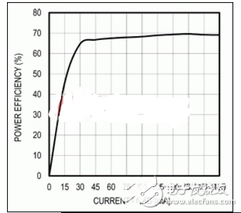
Figure 2.12 Efficiency at the output voltage of V
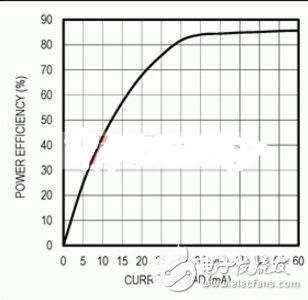
Figure 3.15V Efficiency at Output Voltage
The output noise is well controlled to within 0.5% of the output voltage, and the noise is mainly derived from the switching pulses of the MAX256.
3.3v boost to 12v circuit diagram (3)MC3406A is a new type of single-chip buck-boost DC-DC converter integrated circuit with input voltage of 3~40V, adjustable output voltage, output switch current up to 1.5A, temperature compensated reference voltage source, current limit Features. The integrated circuit can be combined with a small number of external components to form a step-up, step-down, and voltage-reversed DC-DC converter, which can be widely used in various portable instruments and meters.
The MC3406A is used as a step-up DC-DC converter circuit:
LTC1872 is a current mode step-up DC/DC controller with an operating frequency of 550KHz, an input voltage range of 2.5V~9.8V, and a load current of up to 2A. The picture shows a 3.3V to 5V boost converter circuit. Applications include 1 and 2 cell-powered portable devices such as PDAs, GPS systems and board-level boost converters for network systems.
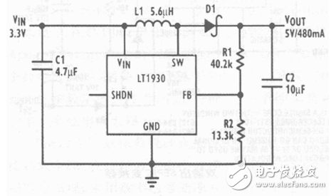
The device's high operating frequency reduces the value and size of inductors and capacitors, allowing the design to be packaged in an area of ​​less than 110mm2. 270μA low operating current, 8μA shutdown current and up to 90% efficiency help extend battery life. The LTC1872 guarantees an output voltage accuracy of ±2.5%. The output voltage is limited only by the performance of the external components. To prevent the N-channel MOSFET from operating below the safe input voltage level, the device has undervoltage lockout characteristics. When the input supply voltage is below 2V, the N-channel MOSFET and controller are turned off, and the undervoltage circuit is still working (it only consumes a few microamps).
3.3v boost to 12v circuit diagram (5) 3.3V to 5V/1A boost to converter circuit
The main features of the LTC3401 and LTC3402 are: up to 3MHz switching frequency, 97% efficiency, and inputs less than 1V. They provide the highest power density for a single-synchronous boost converter, providing up to 5W of regulated output in only 0.05in2. Their miniature size, high efficiency and wide output current range are ideal for application requirements for pagers, cordless phones, GPS receivers and handheld instruments.
To achieve high efficiency, each switching regulator includes a 0.16Ω N-channel MOSFET switching transistor and a 0.18Ω synchronous rectifier. The LTC3402 can deliver up to 1A of load current (2A switching current) with 95% efficiency and 38μA power consumption (operating in BurstMode). The LTC3401 is a similar device with 500mA output capability.
Programmable 300KHz~3MHz switching frequency with a timing resistor to achieve optimum RFI rejection and maximum efficiency. To improve switching harmonic rejection in sensitive audio and IF bands, the LTC3401 or LTC3402 oscillators can synchronize external clocks. BurstMode operation is disabled during synchronization or when the MODE/SYNC pin is low to prevent interference from low frequency ripples.
The LTC3401 and LTC3402 are designed to start at an input voltage of 0.85V (typical). Once started, the IC works by Vout instead of Vin. At this point, the internal circuitry does not depend on the input voltage and thus does not require a large input capacitor. The input voltage can drop below 0.5V without affecting operation, so that the supply can provide enough energy at low voltages.
The left end of the figure is connected to the 3.3V CMOS level, which can be an IO port of STM32, FPGA, etc., and the output of the right end is 5V level, achieving conversion from 3.3V to 5V.
Now let's analyze the role of each resistor (the core idea of ​​grabbing is that the Vbe of the triode is constant at around 0.7V):
Assuming no R87, when the high level of US_CH0 is directly added to the BE of the triode, where is the voltage of 0.7V going?
Suppose there is no R91. When the state of US_CH0 is uncertain, the default is to output high or low level of Trig? Therefore, R91 functions as a fixed level. At the same time, if there is no R91, just turn on the triode by inputting “0.7Vâ€, the threshold voltage is too low, and R91 has the function of raising the threshold voltage (refer to the second section for the analysis of the buzzer).
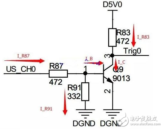
However, adding R91 should pay attention to it: if R91 is too small, the base voltage is similar.
Only when Vb"0.7V can make US_CH0 turn on when it is high. Vb=1.36V in the above figure
Suppose there is no R83. When the input US_CH0 is high (when the transistor is turned on), D5V0 (5V high level) is directly added to the CE level of the triode, and the CE and triode of the triode are easily damaged.
Further analysis of its working mechanism:When the input is high, the transistor is turned on, and the output is clamped to the Vce of the triode. The test result for the circuit is only 0.1V.
When the input is low, the transistor is not conducting, and the output is equivalent to pulling up the input of the next-stage circuit using a 10K resistor. The actual test result is 5.0V (no-load).
Draw-wire sensors of the wire sensor series measure with high linearity across the entire measuring range and are used for distance and position measurements of 100mm up to 20,000mm. Draw-wire sensors from LANDER are ideal for integration and subsequent assembly in serial OEM applications, e.g., in medical devices, lifts, conveyors and automotive engineering.
Linear Encoder,Digital Linear Encoder,Draw Wire Sensor,1500Mm Linear Encoder
Jilin Lander Intelligent Technology Co., Ltd , https://www.landerintelligent.com