
The geological detection system uses 32-bit floating point TMS320C6713 as the controller. With its highly optimized processor structure and unique command system, the ADS1256 collects data for efficient real-time control, analysis and processing.
Chip introductionThe internal structure of the ADS1256 is shown in the figure below. The device is mainly composed of analog multiplexer (MUX), input buffer (BUF), programmable gain amplifier (PGA), fourth-order Δ-modulator, programmable digital filter. Clock generator, controller and serial SPI interface. It is suitable for collecting geological detection systems with a maximum frequency of only a few kilohertz. The data output rate can be up to 30K sampling points per second (SPS), and there is a perfect self-calibration and system correction system. The fixed-point and floating-point operations of 2400MIPS/1800MFLOPS integrate two multipliers on-chip, and the computing power reaches 600MMACS. In this system, multi-channel AD acquisition is adopted. Therefore, TMS320C6713 can greatly meet the real-time requirements of signal processing. And TMS320C6713 has two independent MCBSPS ports, which can be configured to read, write and control the SPI port and ADS1256.
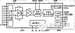
ADS1256 internal structure diagram
DesignWe use multiple ADS1256s to work in parallel in the system. Each ADC shares the system clock, ensuring that each ADC simultaneously samples the inputs. In order to collapse the hardware interface, there is only one interrupt pin in the system. Only the schematic diagram of the DSP and one of the ADCs is given here. The ADS1256 communicates with the DSP's Multichannel Buffered Serial Port (MCBSP) via the SPI serial digital interface.
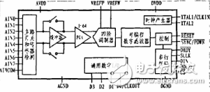
System schematic
DSP and ADS1256 interface design 1. ADS1256 design pointsThe design points of the ADS1256 mainly include internal parameter settings and serial port configuration. The ADS1256 working process is mainly established by setting 11 independent registers. These registers include all the information that needs to be set, such as sampling speed, analog multiplexer, PGA setting, I/O selection, self-calibration, etc. Table 1 shows the main register states of ADS1256, including: status register s, rAll7S, analog multiplexer register MUX, ADTMS320C6713 realizes control register ADCON and data speed register DRATE at 300MHz clock frequency.
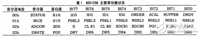
Table 1 ADS1256 main register status
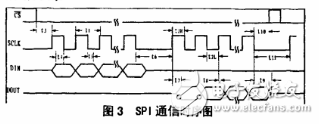
The ADS1256 uses a four-wire system (clock signal line SCLK, data input line DIN, data output lines DOUT and /CS) for SPI communication. The ADS1256 can only work in the slave mode of SPI communication. The design can use the DSP to control the registers on the ADS1256 chip and read and write these registers through the string EL. When serial communication, you must keep /CS low. The DRDY pin is used to indicate if the conversion has been completed, and DRDY is low to indicate that the conversion has been completed. In the SPI communication process, data can be sent and received synchronously, and the data can also be synchronously moved by SCLK and DIN, DOUT signals. The SCLK signal should be kept as clean as possible to avoid data errors. On the falling edge of SCLK, it can be DIN to ADS1256. The data is sent, and on the upper edge of SCLK, data can be read from the ADS1256 via DOUT. Figure 3 shows the SPI communication timing relationship.
There are two multi-channel buffered serial ports (MCBSP) in the TMS320C6713, which is a synchronous serial interface that supports multiple communication methods and SPI protocols. The SPI protocol is a serial interface protocol for four signal lines, including master/slave modes. Serialization is performed through four interface signals: serial data input, serial data output, shift clock, and slave enable. Communication. MCBSP is compatible with SPI protocol when set to clock stop mode. MCBSP supports two kinds of SPI transmission formats, which can be set by CLKSTP bit operation of register SPCR.
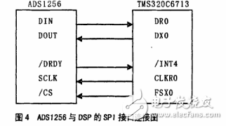
The ADS1256 provides an SPI serial digital interface for flexible and easy communication with the DSP. Figure 4 shows how the ADS1256 can be connected to the DSP. The SPI serial interface of the ADS1256 operates in slave mode, the serial clock (SCLK) of the SPI is supplied by the DSP, and the SPI communication is valid when the chip select signal (/CS) is low. The data valid signal (/DRDY) is used to indicate whether the data conversion is complete. It is high during the data conversion process. When the data result is valid, it becomes low level. Therefore, the signal is often input with an interrupt of the DSP (/ INT) is connected so that the DSP can respond in time to read the converted data. It is worth mentioning that the /DRDY signal is also in a high state when the operating parameters of the ADC change or are being corrected, and after the reset, until the conversion data is valid again. All commands controlled by the DSP to the ADS1256 are sent to the ADS1256 via the data input (DIN) of this SPI serial interface. Inside the ADS1256 there are a series of registers that control the specific operating parameters of the ADC. The various commands sent from the SPI interface indirectly control the working state of the ADS1256 by controlling and changing the value of the corresponding register. Of course, there are some specific characters to use as command words.
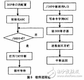
3. software designFirst, the configuration of the TMS320C6713 serial port and the setting of the ADS1256 communication data, the serial communication word module is shown in Figure 5. The DSP internally generates a 1MHz serial port clock, and the serial communication word length is 32 bits, which are respectively 8 bit instruction bytes and 24 bit data bytes. The frame sync signal FSXO is set to active low and is generated by a CLKR0 before each serial communication word is transmitted. Both the FSXO and the data are clocked out on the falling edge of CLKR0 for one serial clock cycle, so that the ADS1256 is effectively sampled on the rising edge.
Toggle Switches,Waterproof Toggle Switch,Waterproof Rocker Switch,Mini Toggle Switch
Lishui Trimone Electrical Technology Co., Ltd , https://www.3gracegfci.com