
Switching power supply has been widely used in many fields such as computer, communication, household appliances, radar, space technology, etc. due to its advantages in volume, weight, efficiency and reliability. Switching power supply control mode: pulse width modulation (PWM), pulse frequency modulation (PFM), pulse width frequency modulation (PWM-PFM). Among them, PWM is the most widely used control method in switching power supply. It has the advantages of low noise and high efficiency at full load. PFM has the advantage of low static power consumption. In many applications, a single PWM or PFM can no longer meet the design needs, but there is currently no dedicated PWM-PFM integrated chip on the market. This paper takes SG3525 as an example to introduce the ideas and methods of implementing variable frequency control with PWM control chip.
1. Introduction to the basic principle of SG3525 and calculation and analysis of PWM pulse frequencyAs shown in Figure 1, the SG3525 is mainly composed of a reference voltage regulator, an oscillator, an error amplifier, a PWM comparator and a latch, a phase splitter, a NOT gate circuit, and a totem output circuit. Pin 16 is the reference voltage source output of SG3525, the accuracy can reach (5.1±1%)V, temperature compensation is adopted, and overcurrent protection circuit is provided. The SG3525's oscillator generates sawtooth oscillations through an external time base capacitor and resistor, and generates a clock pulse signal whose pulse width corresponds to the falling edge of the sawtooth wave. The clock pulse is used as a trigger signal of a phase splitter composed of a T flip-flop to generate a square wave signal with a phase difference of 180°. The error amplifier is a two-stage differential amplifier with a DC open-loop gain of around 70dB. The differentially amplified signal and the sawtooth wave voltage output by the oscillator are respectively applied to the inverting input terminal and the non-inverting input terminal of the PWM comparator, and the modulated signal outputted by the comparator is latched as an input signal of the NOR circuit.
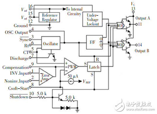
Figure 1 SG3525 internal structure
The final stage of the output uses a push-pull output circuit with a current sink and sink current peak of 200mA. Due to the open-close hysteresis, overlapping conduction occurs between the output and the absorption. There is a current spike at the overlap for a duration of approximately 100 ns. A voltage of about 0.1 μF can be connected to the pin at 13 to filter out the voltage spike.
The pulse frequency of the PWM of SG3525 is determined by the sawtooth frequency of the oscillator. The frequency of each PWM is half of the sawtooth frequency. The pulse width is controlled by the output voltage of the error amplifier. The higher the output voltage of the error amplifier is, the larger the pulse width is. The maximum pulse width is the sawtooth rise time tp (sawtooth period T, dead time td).
All In One Pc 21.5 Inch,All In One Pc Intel Core I5,Intel I5 All In One,Computer All In One Core I7
Guangdong Elieken Electronic Technology Co.,Ltd. , https://www.elieken.com