
Abstract: Combining the advantages of digital frequency synthesizers (DDs) and integrated phase-locked loops (PLLs), high-resolution, low-spur, wide-band frequencies composed of DDS chip AD9954 and integrated phase-locked chip ADF4113 are developed and designed. The synthesizer and the frequency synthesizer were analyzed and simulated. From the simulation and test results, the frequency synthesizer reached the design goal. The frequency synthesizer has an output frequency range of 594 to 999 MHz, a frequency step of 5 Hz, and a phase noise of -91 dBc/
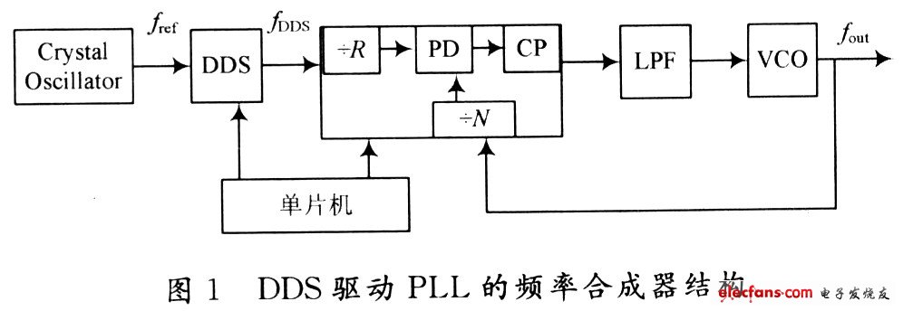
The reference signal of the DDS is generated by a crystal oscillator whose frequency is fref. The signal frequency of the DDS output is fDDS, and the frequency value is controlled by the frequency control word (FTW). The reference signal of the phase-locked loop (PLL) is driven by the output signal of the DDS. The output frequency of the VCO is output by the charge pump (CP) of the PLL chip and is controlled by a low pass filter (LPF). The output signal of the frequency synthesizer is the output signal of the VCO. The frequency synthesizer provides a control signal through the microcontroller to change the division ratio of the FTW and PLL in the DDS.
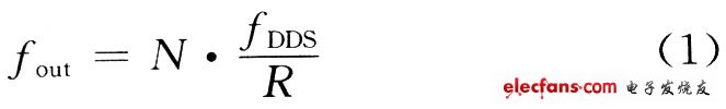
The relationship between the VCO output signal frequency and the DDS output signal frequency is:
The output frequency of the DDS is controlled by the frequency control word K and has:
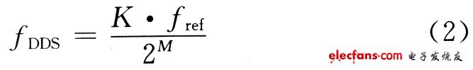
Where: M is the number of bits of the phase accumulator of the DDS; fref is the internal clock of the DDS. Thus, equation (1) can be written as:

In the structure shown in FIG. 1, since the DDS module has a higher frequency resolution, it can be seen from the equation (3) that the theoretical output signal has a higher frequency resolution than the conventional structure. The design has a crystal frequency of 400 MHz and a PLL divider ratio of 27. It can be known from the calculation of equation (3) that the frequency source can achieve a frequency resolution of 5 Hz. The output frequency of the DDS is 22 to 37 MHz, so the system output frequency ranges from 594 to 999 MHz, which meets the design requirements.
L.2 circuit implementation
For the DDS module, the AD9954 chip is used to generate the low frequency reference signal. The AD9954 is the latest AgiIeRF synthesizer from Analog Devices, with a 32-bit frequency control word. At a clock frequency of 400 MHz, the output frequency resolution can reach approximately 4.7 & TImes; 10-5 Hz with a 14-bit programmable phase shifting unit. The chip uses advanced: DDS technology, integrated 14-bit high-performance DAC. The DAC has excellent dynamic performance with phase noise better than -120 dBc/ 
The PLL module is especially important in this design structure. The ADF4113 phase-locked loop chip is used here. The digital phase-locked frequency synthesizer ADF4113 developed by Analog Devices has a maximum operating frequency of 4 GHz and is mainly used in the field of radio frequency to form a digital phase-locked loop to lock a certain frequency. The internal resources of the circuit mainly include programmable analog frequency dividers: 8/9, 16/17, 3z/33, 64/65; programmable 14-bit reference frequency divider; programmable RF signal divider; 3-wire serial bus interface; analog and digital lock status detection. The chip's highest phase-detection frequency is 55 MHz and the chip's noise floor is -171 dBc/ 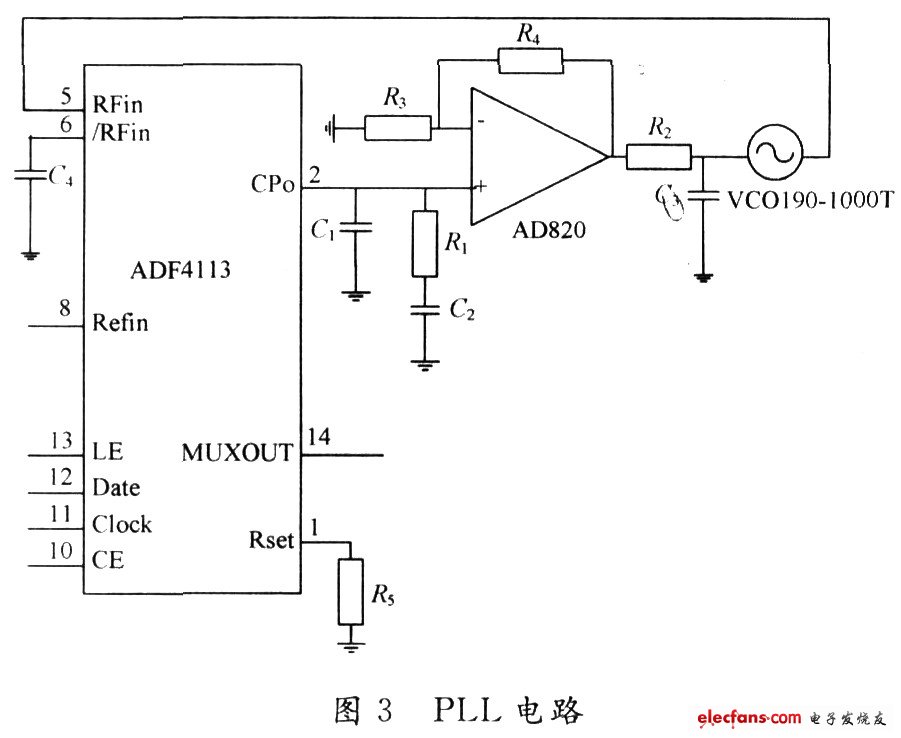
Ejector Header Connector,Dual Row Ejector Header Connector,Single Row Ejector Header Connector,Gold Plated Ejector Header Connector
Shenzhen Jinyicheng Electronci Technology Co.,Ltd. , https://www.jycconnector.com