
Abstract: The Xilinx-based Virtex-II Pro development board implements a dual-core embedded system with shared memory and shared serial output. The construction method and principle of the dual-core system are mainly given. The output of the shared serial port verifies the feasibility of the dual-core system.
With the gradual development of information technology, traditional embedded single-core systems have been unable to adapt to high-performance computing requirements, and FPGA-based dual-core system architecture has gradually developed. Xilinx's Virtex-II Pro development board has a high hardware configuration, manufactured by Digilent, with an XC2VP30 FPGA chip of up to 30,816 logic cells, two hard-core PowerPC405 built into the main chip XC2VP30, and 136 18-bit multiplications. The 2 448 Kbit Block RAM is widely used in universities. However, Xilinx's series of development tools do not support the construction of dual-core on this development board. Xilinx does not provide technical documentation on how to use this dual-core. The Virtex-II Pro development board only has one serial output, which is inconvenient to debug, so domestic. Most university labs are developing applications for the single-core PowerPC405, which does not take advantage of its two hard cores, causing resources to be idle.
In order to make full use of the dual-core resources of the Virtex-II Pro development board, a method for constructing dual-core is proposed. The steps are simple and clear, and the download and debugging are convenient. The output of the shared serial port verifies the feasibility of the dual-core system, and the Virtex II Pro and The development board for the Virtex4 family facing the same problem is also instructive.
1 hardware system constructionThe development tool is EDK9.1i02, and the hardware structure is shown in Figure 1.
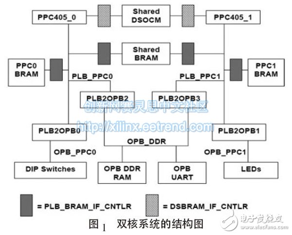
The hardware architecture utilizes two processors, PPC_0 and PPC_1, which share a subset of peripherals, and shared peripherals need to set up shared channels. Each processor can also monopolize some peripherals. PPC_0 controls the peripheral DIP Swiches through the bus bridge. PPC_1 controls the peripheral LED_4Bits, which can verify the working status of each processor. In order to save the program, an exclusive Boot is set for each of the two processors. BRAM and interrupt controller and reset controller. Two PowerPC shared JTAGs can be output through the serial port.
The system design process is as follows:
(1) Using XPS to generate a single core system The system parameters are set as follows:
1System clock: Frequency 100 M, no cache.
2RS232: Baud rate 115200, 8 bits, no interruption.
3DDRAM: 512MB of on-chip memory, no interruption.
4LEDs_4 Bit: No interruption.
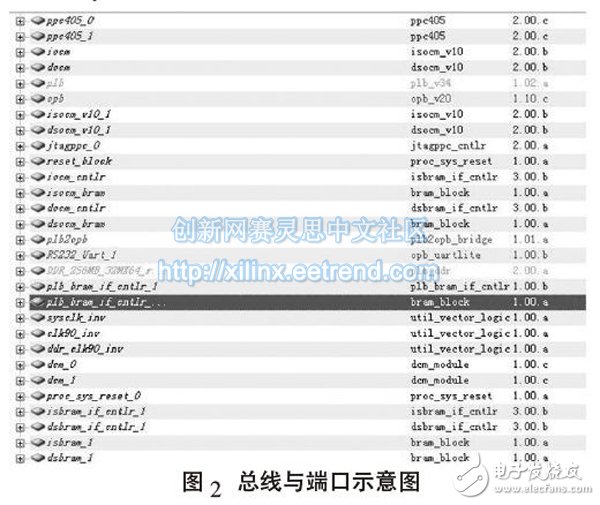
The configured bus and port are shown in Figure 2.
(2) Add PPC405_1 and related settings
1) Setting of PPC405_1 When adding a new IP core PPC405, PPC405_1 has been added to the project along with PPC405_0, but it has not been connected yet. Click Businterface to connect DPLB and IPLB to the PLB bus. Then click -Ports to configure the port of PPC405_1. (By default, there are PLBCLK, BRAMDSOCMCLK, BRAMISOCMCLK. These three ports are not visible. You need to click ConnecTIon Filters to see it.) Add a Reset IP module and select Reset Control-> Processor System Reset Module, which produces a proc_sys_reset_0 module. The value of External ResetAcTIve High in the configuration IP attribute is 0. In order to verify whether the two cores work normally, the UART is used to display the running information for PPC405_0, and the LED is used to display the running information for PPC405_1. Therefore, add an Opb_gpio core with the attribute width of 4 bits and set Channel 1 to Bi-direcTIonal, Channel 1 Input Only is set to FALSE.
2) Configuration of jtagppc_cntlr core
BEGIN jtagppc_cntlr
PARAMETER INSTANCE = jtagppc_0
PARAMETER HW_VER = 2.00.a
BUS_INTERFACE JTAGPPC0 = jtagppc_0_0
BUS_INTERFACE JTAGPPC1 = jtagppc_0_1
END
3) Configuration of shared BRAM core
BEGIN bram_block
PARAMETER INSTANCE = share_bram
PARAMETER HW_VER = 1.00.a
BUS_INTERFACE PORTB=share_bram_if_cntlr_1_PORTA
BUS_INTERFACE PORTA = share_bram_if_cntlr_0_
PORTA
END
(3) Configuration address Assign addresses to peripherals and OCM. For powerpc, ISOCM must fall at the highest end of the address, and DSOCM can be free.
2 Software Engineering Configuration 2.1 Project Construction (1) Configuring the software platform Adding an application to the PPC405_1 is the most critical step, so to compile the PPC405_0 and PPC405_1 separately, that is, modify the Linkerscript (.ld file), a feasible method is: put the startup code and data Place them in two core-independent Isbram_if_cntrl and dsbram_if_ctrl, and put stack and heap in a common bram, such as Plb_bram_if_ctrl.
(2) Add the application project to add the projects ppc0_test_share and ppc1_test_share, respectively to Mark to iniTIalize BRAM, and assign the software project to the respective processors. All the blocks are placed in their own private BRAM, and the Bitstream is updated to generate the corresponding global bit stream. file.
Set the software platform settings for the two cores, and the input and output devices are all equipped with UART, then generate the library and BSP, compile the application, update the bitsream, and finally download the bitsream to the FPGA. The output to the HyperTerminal can verify the correctness of the dual-core configuration. no.
2.2 Interlocking program preparation The interlocking program is modified based on the test program that comes with xilinx. The main modification is to add a program that recognizes the state of the processor. The function is to ensure that the two processors do not interfere with each other. The definition of lwarx.PPC and stwcx .PPC two statements, and in order for the gcc compiler to compile smoothly, write the following code:
#define lwarx (adr) ({unsigned int rval; \
__asm__ __volatile__ (\
" lwarx %0,0,%1" \
: " =r" (rval) :" r" (adr) \
) ;\
Rval;\
})
#define stwcx (adr,val) __asm__ __volatile__ (\
" stwcx. %0,0,%1" \
: : " r" (val) ," r" (adr) \
)
The interlock program indicates the serial port occupancy by the value of the variable Pr_Lock. 0 means idle, 1 means PPC_0 is occupied, 2 means PPC_1 is occupied, and the code segment is as follows:
Volatile int* Pr_Lock = PR_LOCK_ADDR;
Void PRLOCK ()
/* PRLOCK implements a TEST & TEST & SET using the
PPC stwcx and lwarx instructions*/
{
While (1)
{
While (*Pr_Lock ! = 0) ; //wait to release
If (lwarx (Pr_Lock) ! = 0) continue; //latch
Stwcx (Pr_Lock, MY_LOCK_VAL);
If (*Pr_Lock == MY_LOCK_VAL)
{
Sync; // return
Return;
}
Else continue; // retry
}}
Void PRUNLOCK ()
{
// Waiting to empty
While ( XUartLite_mIsTransmitEmpty
(XPAR_RS232_UART_1_BASEADDR) == XFALSE) ;
Sync;
*Pr_Lock = 0;
Return;
}
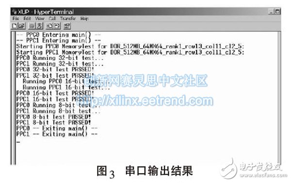
Configure the HyperTerminal, connect the cable, download the cable, and output the bitstream file to the development board. Through the shared serial output, the operating status of both processors can be displayed. The output is shown in Figure 3.
The dual-core system is built on the FPGA development board, which makes full use of the system resources, can properly control the shared peripherals through the interlocking program, and can share a serial port for output, which overcomes the problem of inconvenient debugging. The design method is simple and easy, and the running result proves reliable. The system provides reference value for FPGA-based dual-core embedded system design when the development board manufacturer does not provide relevant information.
Innosilicon Asic Miner:Innosilicon A9 ZMaster,Innosilicon A9++ ZMaster,Innosilicon A9+ ZMaster
Innosilicon is a worldwide one-stop provider of high-speed mixed signal IPs and ASIC customization with leading market shares in Asian-Pacific market for 10 consecutive years. Its IP has enabled billions of SoC's to enter mass production, covering nodes from 180nm to 5nm across the world`s foundries including: GlobalFoundries, TSMC, Samsung, SMIC, UMC and others. Backed by its 14 years of technical expertise in developing cutting-edge IPs and ASIC products, Innosilicon has assisted our valued partners including AMD, Microchip and Microsoft to name but a few, in realizing their product goals.
Innosilicon team is fully devoted to providing the world's most advanced IP and ASIC technologies, and has achieved stellar results. In 2018, Innosilicon was the first in the world to reach mass production of the performance-leading GDDR6 interface in our cryptographic GPU product. In 2019, Innosilicon announced the availability of the HDMI v2.1 IP supporting 4K/8K displays as well as our 32Gbps SerDes PHY. In 2020, we launched the INNOLINK Chiplet which allows massive amounts of low-latency data to pass seamlessly between smaller chips as if they were all on the same bus. With a wide range of performance leading IP in multiple FinFET processes and 22nm planar processes all entering mass production, Innosilicon's remarkable innovation capabilities have been proven in fields such as: high-performance computing, high-bandwidth memory, encrypted computing, AI cloud computing, and low-power IoT.
innosilicon zec miner,Innosilicon A9 ZMaster,innosilicon a9 50ksol miner,innosilicon a9 miner,a9 50ksol zmaster
Shenzhen YLHM Technology Co., Ltd. , https://www.hkcryptominer.com