0 Preface
Integrated operational amplifiers are widely used in the design of electronic circuits, and can perform signal amplification, operation (addition, subtraction, multiplication, division, logarithm, inverse, square, square, etc.), processing (modulation), and waveform generation and Transform. Integrators and filters are two typical application circuits after the op amp is supplemented by peripheral circuits. When the peripheral circuit is more complicated, the characterization of the input / output relationship becomes more cumbersome and difficult. Proteus software has the design and simulation functions of analog circuit, digital circuit and single-chip application system. It is the software that can better simulate the microprocessor at present, and has truly realized the design from concept to product. This article discusses the feasibility of using simulation software to design circuits, and gives typical voltage feedback sampling circuit design methods.
1 Working principle of integrator and filter
1.1 Working principle of integrator
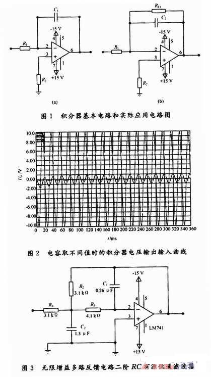
The basic circuit and practical application circuit of the integrator are shown in Figure 1 (a) and (b). The basic circuit input / output voltage relationship of the integrator is as follows:
In practical applications, the feedback capacitor C of the integrator is connected in parallel with the resistor RF, and its input / output voltage relationship is as follows:

When the input power frequency signal amplitude is 5 V, the fixed ratio of RF and R1 is 20 kΩ and 10 kΩ, respectively. Proteus simulation software was used to simulate the input / output with different capacitor values. The results are shown in Table 1 and Figure 2.

It can be seen that when the input frequency is greater than f0, the circuit is an integrator; when the input frequency is less than f0, the circuit is an inverter. The low-frequency voltage gain is:
1.2 Fast filter design
The infinite gain multiple feedback second-order low-pass filter circuit is shown in Figure 3.
The design steps are as follows:
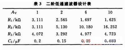
(1) According to the cut-off frequency, select a nominal value of capacitor C from Table 2 to satisfy the following formula:

(2) Find the capacitance value corresponding to AV and the resistance value when K = 1 from Table 3, and multiply the resistance value by K to obtain the design value of the resistance. The basic performance parameters of the filter are Q = 0.707, AV = -R2 / R1.

2 Voltage feedback sampling circuit design
2.1 Filter shift compensation
The filter is an effective measure to improve the power quality, but the phase shift is more complicated to calculate, as shown in equation (5):

In order to overcome the shortcomings, the size of the phase shift can be quickly obtained through software simulation, and accurate data can be provided for the phase shift circuit in the circuit requiring synchronization. The input / output voltage curve of Figure 3 is shown in Figure 4. The amplitude of the input voltage is 5 V and the frequency is 50 Hz.
Commercial Solar Flood Lights,Solar Powered Led Flood Light,Solar Flood Light With Remote Control,200W Solar Flood Lights
Jiangmen Biaosheng Solar Energy Technology Co., Ltd. , https://www.bsprosolar.com
