
There are four typical negative feedback amplifiers. The circuits of other negative feedback amplifiers will have some changes, but they are essentially inseparable from these four typical circuits, so you must master the working principle of these four negative feedback amplifiers.
Voltage parallel negative feedback amplifier
As shown in Figure 5, it is a primary common emitter amplifier, which also constitutes a voltage parallel negative feedback amplifier. In the circuit, VT1 is the amplifier tube, R1 is the collector-base negative feedback bias resistor, R2 is the collector load resistor, Ui is the input signal, and UO is the output signal. Since this is a primary common emitter amplifier, the phase of the VT1 tube collector output signal voltage is opposite to the phase of the input signal voltage at the base.
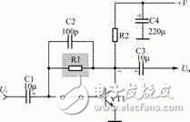
Figure 5 voltage parallel negative feedback amplifier
1 negative feedback component determination method
According to the method of judging that the component connected between the output end of the amplifier and the input terminal may be a negative feedback component, it can be seen from the circuit that it is connected between the base of the input terminal VT1 and the collector of the output terminal VT1. The components have two R1 and C2, so these two components may constitute a negative feedback circuit. The other components are not connected between the input and output of the amplifier, and there is no possibility of forming a negative feedback circuit. Therefore, the focus of the negative feedback circuit is R1 and C2.
2 negative feedback resistor R1 analysis
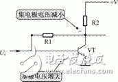
As previously described in the base bias circuit, R1 is the collector-base negative feedback bias resistor of the VT1 tube. Here, the negative feedback process of the circuit after accessing this resistor R1 is explained based on the analysis method of the negative feedback circuit.
Let the signal voltage on the base of the VT1 tube increase at a certain moment, indicated by the + sign. Since the VT1 tube is an NPN type triode, the base current increases as the base signal voltage increases. In addition, since the VT1 tube is connected to the common emitter amplifier, its reverse phase causes the VT1 tube collector output signal voltage to decrease, indicated by the - sign, as shown. The negative output signal voltage is applied to the base of the VT1 tube through the resistor R1, causing the signal voltage on the base of the VT1 tube to decrease, and the signal current at the base of the net input VT1 tube is reduced, so this is a negative feedback process. , R1 is a negative feedback resistor.
The following points are also explained regarding this negative feedback circuit.
The R1 circuit characteristic resistor R1 is connected to the output end (collector) of the amplifier, and the other end is connected to the input terminal (base). Therefore, R1 constitutes a feedback circuit. It is known that the feedback is negative feedback, so R1 is a negative feedback resistor.
Another representation of circuit analysis The working process of this negative feedback circuit can also be described as follows: VT1 tube base signal voltage ↑ → VT1 tube base current ↑ (VT1 is NPN type triode) → VT1 tube collector current ↑ (The collector current is controlled by the base current) → VT1 tube collector signal voltage ↓ (the reverse relationship between the collector signal voltage and current) → VT1 tube base signal voltage ↓ (via resistor R1) → VT1 tube base The current is ↓, so this is a negative feedback process.
Assume that the VT1 base voltage drop analysis method of the negative feedback circuit can also set the VT1 tube base signal voltage to reduce: to set the base signal voltage of a certain VT1 tube ↓ → VT1 tube base current ↓ (VT1 The tube base current subtraction indicates that the negative half-cycle amplitude of the signal is increasing) → VT1 tube collector current ↓ → VT1 tube collector signal voltage ↑ → VT1 tube base signal voltage ↑ (via resistor R1) → VT1 tube base current ↑ (Indicating that the amplitude of the negative half cycle is decreasing, so that the negative half cycle signal of the base of the net input VT1 is decreasing), so this is a negative feedback process.
DC and AC double negative feedback Because the resistor is connected between the base and collector of the VT1 tube, there is no DC-blocking component in the R1 loop, so the current fed back from the collector of the VT1 tube to the base of the VT1 tube can be DC current. It can also be an AC signal current, so the analysis of the above negative feedback process is suitable for both DC and AC, so R1 has a negative feedback effect on both DC and AC signals, and is a DC and AC double negative feedback circuit.
The effect of the negative feedback amount R1 on the negative feedback amount is as follows: when the resistance of R1 is large, the negative feedback signal from the collector of VT1 tube to the base of VT1 tube is small, and if it is large, R1 is open. At this time, no negative feedback signal is applied to the base of the VT1 tube, and there is no negative feedback. Therefore, in this negative feedback circuit, the larger the resistance of the negative feedback resistor R1, the smaller the negative feedback amount, and the larger the gain of the amplifier.
In the troubleshooting, if the amplification of the sense amplifier is slightly worse, it can be solved by a simple method of reducing the negative feedback to improve the amplification capability of the amplifier.
Frequency influence Since the resistor R1 has the same resistance value for the AC signals of different frequencies, there is no selection characteristic for the frequency of the AC signal, so that R1 has the same negative feedback effect on the AC signals of all frequencies.
3 high frequency negative feedback capacitor C2 analysis
It can be seen from the circuit that a small capacitance C2 is also connected in parallel to the negative feedback resistor R1. The analysis of the negative feedback process of C2 is the same as the analysis process of the resistor R1, but the characteristics of the capacitor and the resistor are different. Therefore, the negative feedback principle of this capacitor is different, mainly explaining the following points.
There is no DC negative feedback capacitor with DC blocking function, so the DC voltage on the collector of the VT1 tube cannot be negatively fed back to the base of the VT1 tube through C2, so there is no DC negative feedback in C2.
There is no audio negative feedback VT1 tube is composed of audio amplifier, and C2 has a capacity of only 100pF. Such a small capacitance has a large capacitive reactance to the audio signal and is equivalent to an open circuit. The audio signal cannot be added to the VT1 tube base through C2. Extremely, so C2 does not have negative feedback on the audio signal.
There is only high-frequency negative feedback. C2 has a small capacitive reactance for signals higher than audio, so this high-frequency signal on the collector can be applied to the base through C2, so that C2 is only negative for signals with high frequencies. Feedback effect.
In the amplifier, some high frequency self-excitation phenomenon will occur. Once this high frequency self-excitation occurs, the amplifier will not work normally. For this reason, a high frequency negative feedback capacitor such as C2 is required. Since C2 has a strong negative feedback effect on such a high-frequency signal, the amplifier has a small amplification factor for such a high-frequency signal, thereby achieving the purpose of eliminating the high-frequency self-excitation of the amplifier. In the audio amplifier circuit, a capacitor acting like C2 is called a vibration absorbing capacitor.
4 voltage negative feedback discrimination method
In the circuit, R1 and C2 form a voltage negative feedback circuit, because these two elements feed back the signal voltage of the amplifier to the input of the amplifier, so it is called a voltage negative feedback circuit.
The method for judging this voltage negative feedback circuit is as follows: If the output of the amplifier is shorted to ground, there is no negative feedback in the amplifier, then this is a voltage negative feedback circuit. 4-6 circuit, if the output terminal is shorted to ground, the VT1 tube collector is grounded AC, then the AC output signal UO is equal to zero, R1 has no AC signal applied to the base of the VT1 tube, the circuit does not exist negative Feedback signal, so this is a voltage negative feedback circuit.
5 parallel negative feedback discrimination method
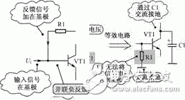
As shown in Figure 5, the parallel negative feedback circuit, the negative feedback signal sent by R1 is added to the base of the transistor after the input signal Ui is connected in parallel with the base, so this is a parallel negative feedback circuit.
When the negative feedback signal is applied from the base of the triode to the input of the amplifier, it is a parallel negative feedback circuit, as shown in Figure 4-7.
Since the negative feedback signals from the input signals Ui and R1 are all added to the triode from the base of VT1, the two signals are in parallel relationship, so they are called parallel negative feedback circuits.
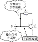
Figure 7 Schematic diagram of judging method of parallel negative feedback circuit
According to the method of voltage negative feedback and parallel negative feedback, R1 and C2 in the circuit shown in Figure 4-5 form a voltage parallel negative feedback circuit.
Shenzhen Sunbeam New Energy Co., Ltd , https://www.sunbeambattery.com