
DC regulated power supply is an important part of modern power electronic systems. A good DC power supply system is an important guarantee for high quality modern electronic systems. Switching power supplies have a wide variety of design methods and complex and diverse methods. Therefore, it is necessary to study a simple method to quickly design the general-purpose high-efficiency, low-cost switching power supply.
1 Switching power supply works
The switching DC stabilized power supply is formed based on the average value of the square wave voltage being proportional to its duty cycle and the integral characteristics of the inductor and capacitor circuits. The basic working principle is that the input AC voltage is first rectified to form a pulsating DC voltage, which is transformed by a DC-DC conversion circuit, and then a high-frequency alternating current of different pulse width is formed by the chopper circuit, and then the rectification and filtering output thereof is required. Voltage and current waveforms. If the output voltage waveform deviates from the required value, a current or voltage sampling circuit performs sampling feedback. After comparing the voltage value with the comparison circuit, the difference signal is amplified to control the pulse frequency f and the duty ratio D of the switching circuit. In order to control the conduction state of the output. Therefore, the output voltage and current can be obtained at the output.
As shown in Figure 1, the switching power supply module is divided into the following sections.
According to the actual needs of the power system, by analyzing each part, the corresponding switching power supply products can be designed.
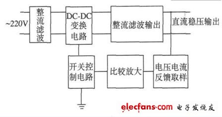
Figure 1 is a block diagram of the switching power supply.
2 Introduction to TopswitchII
TOPSwitch? ? It is a highly integrated dedicated chip for switching power supplies manufactured by POWER. It integrates the power switch tube and its control circuit into a single chip, and has functions such as automatic reset, overheat protection and overcurrent protection. The functional schematic diagram is shown in Figure 2. When the system is powered up, the D pin goes high, the internal current source starts operating and the on-chip switch is at the 0 bit. TOPSwitch charges the capacitor C5 (see Figure 2) connected to the C pin. When the voltage at C5 reaches 5.7 V, the auto-restart circuit turns off and the on-chip switch jumps to 1 bit. On the one hand, C5 provides power to the TOPSwitch internal control circuit to enable the error amplifier to operate, and on the other hand provides a feedback current to control the duty cycle of the switching transistor. The driving signal of the MOSFET switch is jointly generated by the internal oscillating circuit, the protection circuit, and the error amplifying circuit. The higher the voltage across C5, the smaller the duty cycle of the MOSFET switch drive pulse.
3 TOPSwitch chip selection
When designing a switching power supply, first of all, how to choose the appropriate switching power supply control chip. When selecting a chip, it is necessary to meet the requirements without wasting resources due to the selection. The following describes the power loss (PD) and power efficiency (η) and output power (Po) curves of the Topswitch II series switching power supply, and quickly select the model of the chip to complete the design of a universal switching power supply with a wide range of inputs.
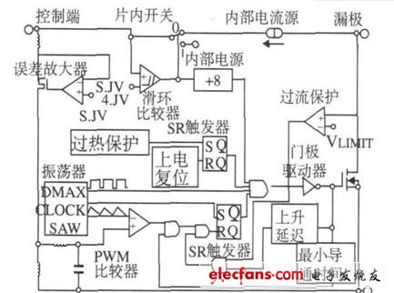
Figure 2 Internal schematic of the TOPSwitch chip.
3.1 PD, η, Po relationship curve
The wide range input AC voltage is 85~ 265 V. Under these conditions, the PD, η, Po relationship curves of the TOP221~TOP227 series single-chip switching power supply are as follows, see Figure 3 and Figure 4.
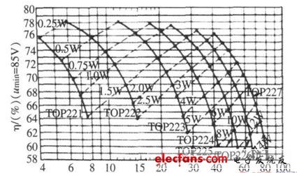
Figure 3 shows the relationship between PD, η, and Po when the input is wide and the output is 5 V. 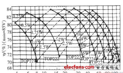
Figure 4 shows the relationship between PD, η, and Po when the input is wide and the output is 12 V.
Note that it is assumed here that the AC input voltage has a minimum value of umin = 85 V and the highest input voltage umax = 265 V. The abscissa on the way represents the output power, while the 15 dotted lines are the contours of the chip power consumption.
First determine the applicable curve. For example, when u= 85~ 265 V, Uo= + 5 V, you should select Figure 3; when u= 220 V (ie 230 V-230 V&TImes; 4.3%), Uo= + 12 For V, you should select Figure 4; then find the power output point P o to be designed on the abscissa; move vertically upward from the output power point, and know the curve that the appropriate chip points. If not, you can continue to look up another solid line; then read the power consumption PD of the chip from the contour (dashed line), and then determine the junction temperature (Tj) of the chip to determine the size of the heat sink.
For example, when designing a 5 V, 30 W general-purpose switching power supply, select Figure 3. Because the universal switching power supply input AC voltage range is 85~ 265 V. First find the output power point of Po = 30 W from the abscissa, then Move vertically upwards, intersect the solid line of T OP224 at one point, find η= 71.2% of the point on the ordinate, and finally find PD = 2.5 W from the contour passing through this point. Select TOP224 to output 30 W power, and the expected power efficiency is 71.2%, and the chip power consumption is 2.5 W. If you feel that the index efficiency is low, you can continue to check the solid line of TOP225. Similarly, the TOP225 can also output 30 W of power, and the expected power efficiency can be increased to 75%, and the power consumption of the chip can be reduced by 1.7 W. Then, according to the obtained PD value, the heat sink design can be completed.
3.2 Correction of equivalent output power
The PD, η, Po relationship curves limit the minimum value of the AC input voltage, umin = 85 V. If the minimum AC input voltage does not meet the above requirements, it will directly affect the correct choice of the chip. At this point must the actual AC input voltage u? The power P'o corresponding to the min minimum is converted to the equivalent power Po when umin is the specified value, and the above graph can be used. The power correction method is as follows: Select the characteristic curve to be used, and then find the conversion coefficient K according to the known u'min value; convert P 'o into the equivalent power Po when umin is the specified value, and express the formula P o=P 'o / K; Then select the appropriate relationship curve from Figure 3, Figure 4.
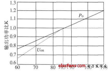
Figure 5 shows the relationship between K and u'min for a wide range of inputs.
For example, design a 12 V, 35 W general-purpose switching power supply, known as umin= 90% &TImes; 115 V = 103.5 V. From Figure 5, find K = 1.15. Bring P 'o = 3.5 W, K = 1.15 into P In o = P 'o / K, Po = 30.4 W is calculated; then according to the value of Po, the best model selected from Figure 4 is the T OP224 chip, where η = 81.6% and PD = 2 W. If T OP223 is selected, η drops to 73.5% and PD increases to 5 W, which is obviously not appropriate. If you choose the T OP225 type, it will waste resources because it is more expensive than the TOP224 and is suitable for outputting more power from 40 to 60 W.
1,2.4G Digital Wireless Backup Camera System for Truck/Van/Caravan/Trailers/Camper/Pickup/5th Wheel/Bus. Easy to install, no more complex wiring.
2, 7-Inch TFT LCD screen Monitor with Built-in Wireless Receiver-- High resolution image and full color display.
3,Rearview IR Reverse HD backup Camera with Built-in Wireless Transmitter---with 12/18/28 individual Infrared (IR) LED for Night Vision. Hard Metal Cased Camera with IP68 Waterproof and Mud proof, Designed and tested for extreme climates.
4, Voltage Range From 12-32V DC Power, Flexible Vehicle Compatibility.
5, Digital wireless technology for specialty vehicles , No any interference with other wireless devices, if you ensure stable and high resolution image with 100M acceptance range in open areas.
Wireless Backup Camera For Car,2.4G Wireless Backup Camera System,Wireless Backup Camera Kit,Wireless Led Backup Camera Kit
Shenzhen Sunveytech Co.,LTD , https://www.sunveytech.com