
System installation and commissioning
Properly arranging system installation and debugging procedures is the key to ensuring efficient and high-quality installation and commissioning tasks. The overall procedure after field inspection and further modification is shown in the figure.
1. Early technical preparation
The more technical preparations before system installation and commissioning, the smoother the installation and commissioning will be. The preliminary technical preparation work includes the following contents:
(1) Familiar with PC random technical data and original data, and deeply understand its performance, function and various operational requirements, and formulate operating procedures.
(2) In-depth understanding of the design data, the system process, especially the process control requirements of the various production equipment should have a comprehensive understanding, on this basis, according to the subsystem to draw the process flow. Cheng Lian lock diagram, system function diagram, system operation logic diagram, which will help to understand the system operation logic, is an important part of the preliminary technical preparation.
(3) Familiar with the performance, design and installation of each process equipment, especially the control and power wiring diagram of each equipment, and compare with the real object, and find errors and correct them in time.
(4) Based on a comprehensive understanding of the design scheme and PC technical data, list the PC input and output point number table (including the internal coil list, I/O location, corresponding equipment and I/O point functions).
(5) Study the program provided by the design, draw timing diagrams on some of the logically complex input and output points, and some logic errors in the design can be found when drawing the timing diagram.
(6) Molecular system preparation debugging plan, and then integrated into a system-wide debugging program based on collective discussion. 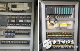
2, PLC commodity inspection
The commodity inspection shall be carried out jointly by both Party A and Party B. The type, quantity and specifications of the equipment and spare parts, spare parts, technical data, accessories, etc. shall be confirmed, and the performance shall be verified by the laboratory and on-site commissioning. The results of the commodity inspection, the two sides should sign the exchange list.
3, laboratory debugging
(1) PLC installation and opening of the metal bracket, the input and output modules of each workstation are fixed on it, and the stations are connected with the host computer, programmer, printer, etc. according to the installation summary, and the wiring is correct. After the power supply level is consistent with the PLC voltage selection, power is sent according to the startup program, the system configuration tape is loaded, the system configuration is confirmed, the programmer loading tape, the programming tape, etc. are loaded, and the system is turned on according to the operating procedure. Conduct various operational tests.
(2) Type the work program
(3) Analog I/O input and output, check and modify the program. The purpose of this step is to verify the correctness of the input working program. The interlocking relationship of the process equipment expressed by the logic of the program is consistent with the design process control requirements. Whether the program is unblocked. If it does not match or can not run to complete the whole process, indicating that the program is wrong, it should be modified. In this process, the understanding of the program will be gradually deepened, ready for on-site debugging, and the irrational and imperfect parts of the program can be found for further optimization.
There are two kinds of debugging methods: 1 simulation method: make a debugging board according to the design, simulate the input node with the toggle switch, simulate the relay and contactor of the production process equipment with small relay, and the auxiliary signal contact return signal node when the auxiliary device is running. The advantage is that it has the authenticity of the simulation, and it can reflect whether a logical malfunction occurs when the on-site mechanical contact with a large difference in switching speed and the electronic contacts in the PLC are connected to each other. The disadvantage is the need to increase commissioning costs and part of the commissioning effort. 2 Forced method: Using the PLC forced function, the mechanical contacts (switches) involved in the program in the program are forced to "pass" and "break" to force the program to run. The advantage is that the debugging workload is small and simple, and no additional cost is required. The disadvantage is that the logic verification is not comprehensive. Manually forcing the analog site nodes to "pass" and "break" will cause the program to run continuously and can only be segmented.
According to the experience of our on-site debugging, the simulation method is adopted for some important on-site nodes, and the rest adopts the forced method, which is complementary to the length of the two.
In the logic verification phase, it is necessary to fill in the commissioning work log day by day, including debugging personnel, time, debugging content, modification records, faults and handling, handover acceptance and signature, to establish a debugging work responsibility system, and leave first-hand information for debugging. For the modification part of the design procedure, it should be indicated on the design drawing, solicit the opinions of the designer in time, and strive to accurately reflect the design requirements.
4. On-site installation and inspection of PLC
After the laboratory commissioning is completed, the equipment is moved to the site for installation after the conditions are ripe. The installation should meet the requirements, the plug-in should be inserted firmly and fastened with bolts; the communication cable should be unified model, can not be mixed, if necessary, the instrument should be used to check the attenuation of the line signal, the attenuation value does not exceed the index proposed by the technical data; the measuring host, I /O cabinet, connecting cable and other grounding insulation resistance; measuring system grounding resistance for grounding; checking the power supply, etc., and making a record, until all the items meet the requirements, can be powered on.
PGA Sockets Pin Grid Array Socket
A pin grid array, often abbreviated PGA, is a type of integrated circuit packaging. In a PGA, the package is square or rectangular, and the pins are arranged in a regular array on the underside of the package. The pins are commonly spaced 2.54 mm (0.1") apart, and may or may not cover the entire underside of the package.
PGAs are often mounted on printed circuit boards using the through hole method or inserted into a socket. PGAs allow for more pins per integrated circuit than older packages, such as dual in-line package (DIP).
PGA Sockets & Adapters
Low insertion force Pin Grid Array (PGA) Sockets and Adapters are available in a variety of RoHS Compliant insulators with hundreds of screw-machined terminal choices. Virtually any PGA footprint can be accommodated, including interstitial patterns.
PGA Sockets & Adapters Overview
Durable construction for virtually any application
Wide variety of materials, lengths, and sizes
Cost-effective method for replacing, repairing, or upgrading PGA devices
Unique options such as solder preform terminals eliminate the need for wave soldering in mixed SMT/Thru-hole applications
RoHS compliant insulators and screw-machined terminals are compatible with lead-free processing - select either Matte Tin/Gold (MG) or Gold/Gold (GG) plating
Antenk's Pin Grid Array (PGA) Sockets
Complex printed circuits are too valuable to risk direct soldering to expensive integrated circuits (ICs). Using a socket is the answer. The use of sockets offers advantages that prove cost effective and simplify board design.
Antenk's processor socket line is designed for use with Intel- and AMD-based microprocessor packages. Socket types include land grid array (LGA), micro pin grid array (mPGA), and PGA with low to zero insertion force. The mPGA and PGA sockets are designed for various microprocessor packages for notebook PCs, desktop PCs, and servers. For custom applications, the compression sockets can be configured to the specific application.
mPGA/PGA (ZIF)These sockets provide a zero insertion force (ZIF) PGA interface to the microprocessor PGA package and are attached to the PCB with surface-mount technology (SMT) soldering. PGA sockets are available in arrays up to 989 positions with single lever, screw driver, and hex wrench actuation methods.
PGA Sockets (LIF)
These sockets are primarily employed for microprocessor package test applications using through-hole solder attachment to the PCB design. The contacts are screw-machine outer sleeves with either stamped and formed or drawn inner contacts. Custom arrays are available in more than 1,000 positions.
Pin Grid Array (PGA) Sockets Type
mPGA
PGA

Eliminate hand-loading of pins, facilitate solder joint visibility, low profile component mounting or board mating.
PGA Sockets,mPGA Sockets,Integrated Circuits Socket,Pin Pga Sockets,Pga Socket Connector,PGA Adapters,Pin Grid Array Sockets,Processor Socket
ShenZhen Antenk Electronics Co,Ltd , https://www.antenkcon.com