

AC input EMI filter
There are usually two ways in which the interference current is transmitted on the wire: common mode and differential mode. Common-mode interference is the interference between the carrier fluid and the earth: the interference is consistent in size and direction, exists between any relatively large ground in the power supply, or the midline to the earth, and is mainly generated by du/dt. The di/dt also produces a certain total Mode interference. The differential mode interference is the interference between the carrier fluids: the interference is equal in magnitude and opposite in direction, and exists between the power line and the neutral line, and between the phase line and the phase line. When the interference current is transmitted on the wire, it can be either common-mode or differential-mode. However, the common-mode interference current only becomes differential-mode interference current, which can interfere with the useful signal.
There are two types of interference in the AC power input line, usually low-band differential mode interference and high-band common mode interference. In the general case, the differential mode interference amplitude is small, the frequency is low, and the resulting interference is small; the common mode interference amplitude is large and the frequency is high, and radiation can also be generated through the wire, resulting in greater interference. If an appropriate EMI filter is used at the input end of the AC power source, electromagnetic interference can be effectively suppressed. The basic principle of the power line EMI filter is shown in Figure 1. The differential mode capacitors C1 and C2 are used to short-circuit the differential mode interference current, while the intermediate connection grounding capacitors C3 and C4 are used to short-circuit the common mode interference current. The Common Mode Choke Coil consists of two coils that are equally thick and wound in the same direction around a magnetic core. If the magnetic coupling between the two coils is very tight, then the leakage inductance will be very small, and the differential mode reactance will become very small in the power line frequency range; when the load current flows through the common mode choke coil, the series connection The lines of magnetic force generated by the coils on the phase lines and the lines of magnetic force generated by the coils connected in series on the neutral line are opposite to each other and they cancel each other out in the magnetic core. So even in the case of large load currents, the core will not saturate. For the common-mode interference current, the magnetic fields generated by the two coils are in the same direction, and they will exhibit larger inductance, which will act to attenuate common-mode interference signals. Here, common mode chokes should use ferrite magnetic materials with high magnetic permeability and good frequency characteristics.
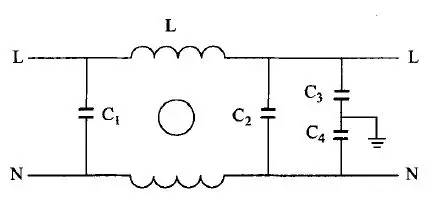
Figure 1 The basic circuit diagram of the power line filter
Use absorption loops to improve switching waveforms
Switching tube or diode in the opening and closing process, due to the presence of transformer leakage inductance and line inductance, diode storage capacitance and distributed capacitance, easy to switch transistor collector, emitter and diode across the peak voltage. RC/RCD absorption loops are usually used. The RCD surge voltage absorption loop is shown in Figure 2.
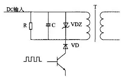
Figure 2 RCD surge voltage absorption circuit
When the voltage on the absorption loop exceeds a certain level, each device rapidly conducts, thereby discharging the surge energy and limiting the surge voltage to a certain extent. A saturable magnetic core coil or microcrystalline magnetic beads are serially connected to the positive electrode lead of the switch collector and the output diode, and the material is generally cobalt (Co). When the normal current is passed, the magnetic core is saturated and the inductance is small. Once the current is to flow in the reverse direction, it will generate a large back-EMF, which effectively suppresses the reverse surge current of the diode VD.
Switching frequency modulation
The frequency control technology is based on the fact that the energy of the switching interference is mainly concentrated on a specific frequency and has a large spectrum peak value. If these energy can be dispersed over a wider frequency band, the purpose of reducing the peak of the interference spectrum can be achieved. There are usually two kinds of processing methods: random frequency method and modulation frequency method.
The random frequency method adds a random disturbance component to the circuit switching interval to disperse the switching interference energy in a certain range of frequency bands. Studies have shown that the switching interference spectrum becomes a continuous distribution of interference from the original discrete spike interference, and its peak value is greatly reduced.
Modulation frequency method is to add a modulating wave (white noise) in a sawtooth wave, forming an edge band around the discrete frequency band that generates interference, and spreading the discrete frequency band modulation of the interference into a distribution band. In this way, the interference energy is spread over these distribution bands. Without affecting the operating characteristics of the converter, this control method can well suppress the interference at turn-on and turn-off.
Soft switch technology
One of the disturbances of the switching power supply is du/dt when the power switch is turned on/off. Therefore, reducing du/dt of the power switch on/off is an important measure to suppress the interference of the switching power supply. Soft-switching technology can reduce the on/off du/dt of the switch.
If a small inductor, capacitor, and other resonant components are added to the switching circuit, an auxiliary network is formed. The resonance process is introduced before and after the switching process to reduce the voltage to zero before the switch is turned on. This can eliminate the phenomenon of voltage and current overlapping in the open process and reduce or even eliminate the switching loss and interference. This circuit is called a soft switching circuit. .
According to the above principle, two methods can be adopted, namely, the current is zero before the switch is turned off, and no loss and interference will occur when the switch is turned off. Such a shutdown mode is called zero current shutdown; or the switch is turned on. If the voltage is zero before the switch is turned on, no loss or interference will occur. This turn-on mode is called zero-voltage turn-on. In many cases, turning off or turning off is no longer indicated, and only the zero-current switch and the zero-voltage switch are called. The basic circuit is shown in FIGS. 3 and 4 .
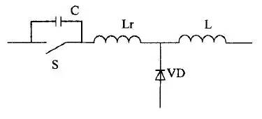
Figure 3 Zero-Voltage Switching Resonant Circuit
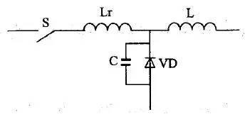
Figure 4 zero current switch resonant circuit
Soft-switching circuit control technology is usually used, combined with reasonable component layout and printed circuit board wiring, grounding technology, to improve the EMI interference of the switching power supply.
Use electromagnetic shielding measures
Generally, electromagnetic shielding measures can effectively suppress the electromagnetic radiation interference of the switching power supply. Switching power supply shielding measures are mainly for switching tubes and high frequency transformers. A large amount of heat is generated when the switch tube is working, and a heat sink is required to be provided to the switch tube, so that a large distributed capacitance is generated between the collector and the heat sink of the switch tube. Therefore, an insulating shield metal layer is placed between the collector and the heat sink of the switch tube, and the heat sink is connected to the shell ground. The metal layer is connected to the zero potential of the hot end, so that the coupling capacitance between the collector and the heat sink is reduced, thereby reducing the Radiator radiation interference. For high-frequency transformers, the structure of the magnetic conductor should first be selected according to the shielding properties of the magnetic conductor. If a can core and an El core are used, the shielding effect of the magnetic conductor is very good. When the transformer is shielded, the shielding box should not be tightly attached to the outside of the transformer. There should be a certain air gap. If a multi-layered shield with an air gap is used, the resulting shielding effect will be better. In addition, in high-frequency transformers, it is often necessary to eliminate the distributed capacitance between the primary and secondary coils. Along the entire length of the coil, an open-loop ring made of copper foil can be interposed between the coils to reduce the number of problems. Together, this open circuit band is connected to the core of the transformer, and it is also connected to the ground of the power supply, which acts as an electrostatic shield. If the conditions permit, the entire switching power supply is equipped with a shield, which will better suppress radiated interference.

Within 1MHZ with differential mode interference
1 150KHZ-1MHz, mainly in differential mode, 1-5MHz, differential mode and common mode work together, after 5MHz is basically common mode. Differential mode interference and inductive coupling. Generally, interference above 1 MHz is common mode, and low frequency band is differential interference. Using a resistor string capacitor and then to the Y capacitor pin, using the voltage of the oscilloscope to measure the resistance of the two pins can estimate the common mode interference;
2 after the insurance plus differential inductance or resistance;
3 Low-power power supply can use PI filter processing (It is recommended that the electrolytic capacitor near the transformer can be used larger).
4 The differential mode inductance in the front-end π EMI part is only responsible for low-frequency EMI, and the volume selection is too large (DR8 is too large, and resistance type or DR6 can be used better) Otherwise, the radiation is not good, if necessary, beads can be strung, because Frequency will fly directly to the front end will not follow the line.
5 When the conductor is cold, it will exceed the standard at 0.15-1MHZ. When there is a thermal engine, there will be 7DB margin. The main reason is that the primary BULK capacitor DF value is too large, the cooler ESR is relatively large, the heat engine ESR is relatively small, the switch current in the ESR formed on the switching voltage, it will be pressed in a current LN line flow, this is the differential mode interference. The solution is to use a low ESR electrolytic capacitor or a differential mode inductor between two electrolytic capacitors.
6 test 150KHZ total solution: increase the X capacitor to see if it can not come down, if it shows that the differential mode interference. If it does not have much effect then it is common-mode interference, or if the power line is wound a few times on a large magnetic ring, it means common-mode interference. If the interference curve is well behind, decrease the Y-capacitance and see if the board has any problems, or add a magnetic ring in front of it.
7 It is possible to increase the inductance of the single winding inductance of the PFC input section.
8 The components in the PWM line adjust the main frequency to about 60KHz.
9 Use a piece of copper skin close to the transformer core.
10 The common-mode inductance has asymmetrical inductance on both sides, and a few turns on one side can also cause conduction exceeding 150KHZ-3MHZ.
11 The general conduction has two main points: about 200K and 20M, these points also reflect the performance of the circuit; about 200K is mainly the spike caused by leakage inductance; about 20M is mainly the noise of the circuit switch. Dealing with bad transformers will increase the amount of radiation, plus shielding is useless, radiation can not be.
12 Change the input BUCK capacitor to a low internal resistance capacitor.
13 For non-Y-CAP power supply, winding the transformer first winds up the primary, then the auxiliary winding and the auxiliary winding tightly around one side and then the secondary winding.
14 Connect a common-mode inductor in parallel with a few K to tens of K resistors.
15 After the common mode inductor is shielded with copper foil, it is connected to the ground of a large capacitor.
16 In the PCB design, the common mode inductor should be separated from the transformer to avoid mutual interference.
17 condom magnetic beads.
18 The three-wire input reduces the capacity of the Y-ground capacitance of the two incoming lines from 2.2nF to 471.
19 For the two-stage filtering, the 0.22uFX capacitor of the rear stage can be removed (sometimes the front and rear X capacitors will oscillate).
20 For the π-type filter circuit, there is a BUCK capacitor lying on the PCB and close to the transformer. This capacitor interferes with the L channel of the conduction 150KHZ-2MHZ. The improved method is to use copper mooring to shield the capacitor to ground, or use A small PCB separates this capacitor from the transformer and PCB. Or stand up this capacitor and use a small capacitor instead.
21 For the π-type filter circuit, there is a BUCK capacitor lying on the PCB and close to the transformer. This capacitor has interference to the L channel of the conduction 150KHZ-2MHZ. The improved method is to use this capacitor with a 1uF/400V or 0.1uF/400V capacitor. Instead, increase the other capacitor.
22 Add a small, several hundred uH differential mode inductor in front of the common mode inductor.
23 The switch tube and the heat sink are wrapped in a length of copper foil, and both ends of the copper foil are short-circuited together, and a copper wire is connected to the ground.
24 Wrap the common mode inductor with a copper piece and connect it to the ground.
25 Connect the switch tube with metal and connect it to the ground.
26 Increasing the X2 capacitance can only solve the frequency band around 150K, and cannot solve the frequency band above 20M. Only the power input is provided with a level 1 nickel-zinc ferrite black magnetic ring, and the inductance is about 50uH-1mH.
27 Increase the X capacitance at the input.
28 Increase input common mode inductance.
29 Reverse the auxiliary winding supply diode to ground.
30 Change the auxiliary winding supply filter capacitor to a thin elongated electrolytic capacitor or increase the capacity.
31 Increase the input filter capacitor.
32 150KHZ-300KHZ and 20MHZ-30MHZ However these two are conductive, can be added prior to a differential mode circuitry common mode circuitry. You can also see if there is a problem with the ground. The ground must be reinforced and the ground on the motherboard must be straightened. The traces between different grounds must be smooth and not staggered.
33 In the rectifier bridge and capacitor, when considering the common mode component, it should be adjacent to the capacitor, when considering the differential mode component, it should be diagonal and capacitance.
34 Increase the input differential mode inductance.
1MHZ---5MHZ differential mode common mode mixing
A series of X capacitors are connected in parallel with the input to filter out the differential interference and analyze which interference is exceeded and resolved.
1 For the differential mode interference can be adjusted X capacitance, add differential mode inductors, adjust the differential mode inductance.
2 Common mode interference can be added for common mode interference, and a reasonable amount of inductance can be used to suppress it;
3 It is also possible to change the characteristics of the rectifier diode to handle a pair of fast diodes such as the FR107 pair of normal rectifier diodes 1N4007.
4 For power supplies with Y capacitors, the interference is dominated by differential mode before 1M, and 2-5M is differential mode and common mode interference. For NO-Y, the situation is not the same, and the common model before 1M is also very powerful. In front of a lot of X capacitors, filter differential mode, change does not change the transformer has no effect on the differential mode, if there is a change, is a common mode. Differential common-mode separation method: Add a lot of X-capacitors to the AC input, from small to large, so that you can filter the differential mode, the rest is common mode, and then compared with the total noise, you can see the difference mode size.
5 When winding the transformer, put all the same names on the side to reduce the 1.0MHZ-5.0MHZ conduction interference.
6 For low-power two differential-mode inductors, reducing the number of differential-mode inductor turns can reduce the conduction 1.2 MHz interference.
7 Increase the Y capacitor to reduce the 1MHZ-5MHZ interference in the middle of conduction.
8 For a switching power supply without a Y-capacitor, EMI exceeds 1MHZ-6MHZ. If the EM drops after adding a Y-capacitor, then several layers of adhesive tape can be added between the primary and secondary transformers.
9 Connect the MOSFET heat sink to the MOS S pole.
10 Connect the small-capacity high-voltage ceramic chip or high-voltage chip capacitor in parallel with the input filter capacitor.
5M---20MHZ is mainly based on common touch interference and adopts the method of suppressing common touch.
1 For the grounding of the enclosure, using a magnetic ring around the ground for 2-3 turns will have a greater attenuation effect on the interference above 10 MHz;
2 Select the copper foil sticking to the core of the transformer. The copper foil should be closed.
3 The size of the shunt capacitor of the primary output circuit and the absorption circuit of the back-end output rectifier is processed.
4 Use a very thin triple insulated wire on the primary winding of the transformer and wrap around a shield winding. Connect one end of the shield winding to the power supply and the other end to the ground through a capacitor.
5 The common mode inductance can be changed to one side of the number of turns more than the other side, and the other has the role of differential mode.
6 Add a small heatsink to switch D and connect it to the negative side of the high voltage terminal. Connect the primary start of the transformer to the D pole of the MOS transistor.
7 Connect the secondary heat sink with a 102 Y capacitor to the primary L/N line to reduce the conducted interference.
8 If you increase the Y capacitor conduction interference down, you can change the transformer winding to improve, you can add more layers of tape between the primary and secondary; if you increase the Y capacitor conduction interference is not improved, you must change the circuit can be changed without changing Transformer winding.
9 Increase the transformer inductance appropriately to reduce the conduction interference of the RCC switching power supply at half load.
10 Use the transformer secondary auxiliary winding to shield the primary primary winding. It is much better to conduct the shielding of the primary primary winding than to use the primary auxiliary winding of the transformer.
11 The overall conduction is excessive. Use an oscilloscope to see that the G and D pole waveforms of the switch tube overlap each other. The output impedance of the light switch from the output filter common mode inductor to the output positive terminal is not changed after passing through a large current.
12 In the input end, L line and N line are each connected to a 681/250V Y capacitor. The Y capacitor is connected to the secondary ground at the other end.
13 The secondary auxiliary winding is used to shield the primary main winding, which can reduce the conduction 3-15MHZ interference. It is much better to shield the primary primary winding with the secondary auxiliary winding than to shield the primary primary winding with the primary auxiliary winding.
14 Put a layer of copper on the bottom of the PCB board to connect the primary capacitor negative electrode.
15 Wrap the entire power supply with a piece of copper, and connect the copper to the cathode of the primary bulk capacitor.
16 Reduce the Y capacitor capacity.
For 20--30MHZ
1 for a class of products can be used to adjust the Y2 capacitance or change the Y2 capacitor position;
2 Adjust the Y1 capacitor position and parameter value between the secondary sides;
3 In the copper foil outside the transformer, the inner layer of the transformer is added with a shielding layer, and the arrangement of the windings of the transformer is adjusted.
4 Change PCB LAYOUT;
5 output line in front of a small double-wire winding around the common mode inductance;
6 Connect the RC filter at both ends of the output rectifier parallel and adjust the reasonable parameters;
7 Add magnetic beads between transformer and MOSFET;
8 Add a small capacitor to the input voltage of the transformer.
9 can increase the MOS drive resistance.
10 may be caused by an electronic load, and resistance loads may be used instead.
11 MOS transistor D can be connected to a 101 capacitor by ground.
12 The output rectifier diode can be replaced by a smaller product capacitor.
13 The RC circuit of the output rectifier diode can be removed.
14 Add two Y capacitors to ground at the input to reduce conduction 25MHZ-30MHZ interference.
15 Apply a copper sheath to the magnetic core of the transformer. The copper sheath is connected to the ground.
16 After the conduction 25MHZ exceeds the limit, a common mode inductance may be added at the output end, and a long magnetic force suitable magnetic Bead may be placed on the switch source detection resistor.
EMI's actual rectification strategy after switching power supply design - radiation part
30---50MHZ is generally caused by high-speed turn-on and turn-off of MOS transistors.
1 can increase the MOS drive resistance;
2 RCD buffer circuit uses 1N4007 slow tube;
3 VCC supply voltage is solved with 1N4007 slow tube;
4 or the front end of the output line is connected in series with a small double-wire and small common-mode inductor;
5 Connect a small absorption circuit in parallel with the DS pin of the MOSFET;
6 Add the BEAD CORE between the transformer and MOSFET;
7 Add a small capacitor to the input voltage of the transformer;
8 PCB core LAYOUT large electrolytic capacitors, transformers, MOS circuit loop as small as possible;
9 Transformers, output diodes, and output flat-wave electrolytic capacitors form a circuit loop that is as small as possible.
50---100MHZ is generally caused by the reverse recovery current of the output rectifier.
1 can be stringed on the rectifier ball;
2 Adjust the absorption circuit parameters of the output rectifier;
3 can change the impedance of the secondary-side Y-capacitance branch, such as the PIN pin plus the BEAD CORE or series resistors in place;
4 can also change the MOSFET, the radiation output rectifier diode body into space (such as iron clamp MOSFET; iron clip DIODE, change the radiator ground point).
5 increase shielding copper foil to inhibit space radiation.
Above 200MHz, the switching power supply has a small amount of basic radiation, and it can generally pass EMI standards.
Switching Power Supply EMI Countermeasures
1 external structure shielding treatment;
2 external cable processing;
3 product internal cable processing;
4 PCB layout processing;
5 switching power supply oscillation frequency selection;
6 IC model selection;
7 selection of magnetic material frequency and bandwidth;
8 transformer selection, winding and design;
9 Radiator grounding method.
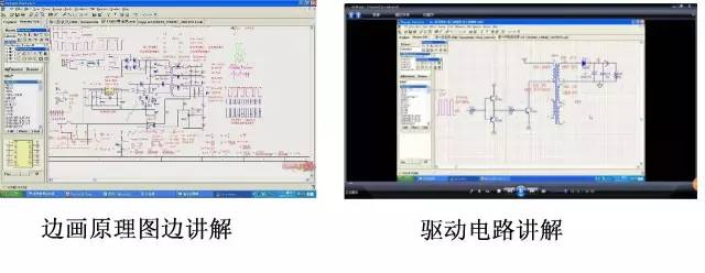
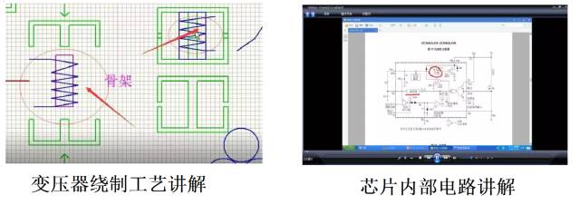
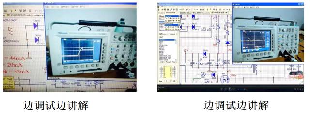
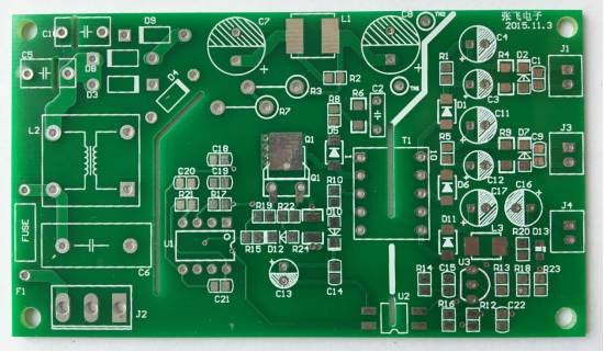
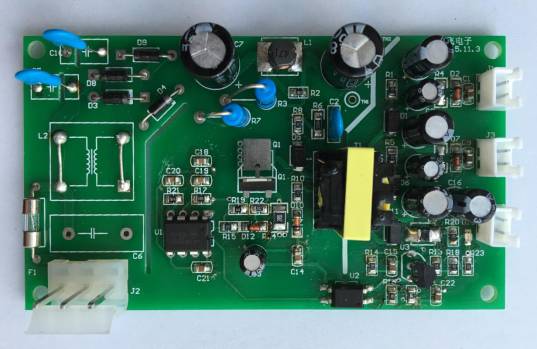
Based on the actual project, the original flyback switching power supply video tutorial exposure
In order to provide a learning platform for newcomers who would like to learn the power technology and find no way to further consolidate the power supply technology, this well-known senior power engineer Zhang Fei invited the power development elite circle to spend a full six months to do it. A real project of flyback switching power supply, recorded the entire project process as a video; explained it while doing the project, and recorded it at the same time.
Video content screenshot mysterious exposure
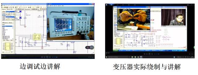
PCB version, power real exposure
Our company`s current transformers have high precision,wide range,small volume and good linearity that can be used to the field of electronic watt-hour meter, electric energy metering, electronic detection.
Performance
â—Power frequency insulation strength:The insulation between the primary winding and the secondary winding and the ground part of the CT can bear 4kV power frequency voltage for 1minute
â—Interturn insulation strength:The secondary open circuit, the primary winding through the rated current 1min, no inter-turn damage in the transformer
â—The deviation is better than the industry standards and national standards
Ct Current Transformer,General Type Current Transformer,New Current Transformer,Latest Voltage Transformer
Anyang Kayo Amorphous Technology Co.,Ltd. , https://www.kayoamotech.com