
Switching power supply electromagnetic interference prevention technology - Conduction articles Preface Power supply products in the verification, often encounter electromagnetic interference (EMI) problems, sometimes it takes a lot of time to deal with, many engineers are also in response to electromagnetic interference Experience is more important than theory, knowing which frequency band to counter those components, but theoretical analysis is lacking. The author has been engaged in the design of switching power supply for many years and hopes to be able to organize the experience and related theoretical basis of the previous countermeasures, so that those who are currently engaged in or want to engage in switching power supply design can have a preliminary understanding of the electromagnetic interference control technology.
The electromagnetic interference test of switching power supply can be divided into conduction test and radiation test. The conduction test frequency band of general switching power supply is between 150K~30MHz, and the frequency band of radiated interference is 30M~300MHz. After 300MHz, the frequency band is generally not a power supply. Produced, so most can be ignored.
The following sections include chapters on conduction test regulations, test and measurement methods, basic concepts, filter design for suppression of conducted interference, and wiring and transformer design.
2 Regulations for the Conduction of Conducted Regulations Regulations Due to product differences, the applicable provisions are also different. Generally, they use the European EN-55022 or the United States FCC part15 to define the limit line, which can be divided into CLASS A and CLASS. B two standards, CLASS A for products used in commercial and industrial areas, CLASS B products for use in residential and home areas, the author designed the product for the 3C home power supply, conduction test frequency band of 150K ~ 30MHz, before product testing Please confirm the safety of the application first, and there will be different standard lines for different safety regulations and ratings.
Figure 1 is an example of the EN-55022 CLASS B limit line diagram, the red line is the limit line (QP, Quasi-peak), pink is the average (AV, Average) limit line, the ultimate goal of the conduction test, The test machine can be completely below its limit line, whether it is QP value or AV value; generally when applying for safety, although only apply below the limit line, most of them will do less than 2dB error. Prevent the difference caused by the test site, and the client sometimes requires less than 4~6dB to prevent the error after the mass production of the product.
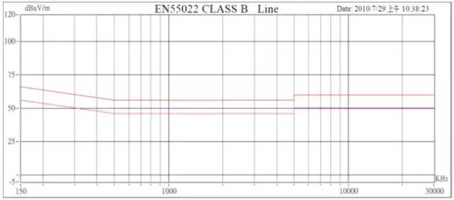
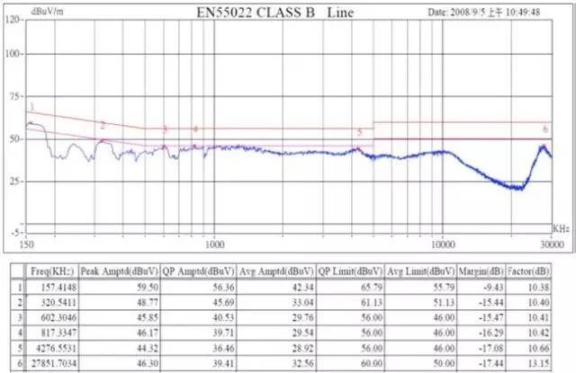
Figure 2 shows an example after measurement. The peak measurement is used for general measurement. The peak measurement is the simplest and fastest method. The measurement instrument is a unit of 9KHz and is used between 150K and 30MHz. The maximum value (maximum hold) is used to obtain the peak reading of the conduction. Use this to confirm the maximum peak value of the power supply and then use this to grab the actual QP and AV values ​​of the highest peak to reduce the scan time. The blue curve in Figure 2 is The quasi-peak peak measurement results are generally measured after the peak measurement, and then the quasi-peak (QP) and average (AV) measurements are performed on the higher six frequency points, as shown in FIG. 2 .
The difference between peak value and quasi-peak value is that the peak value is measured in the receiver's reading in the maximum value regardless of the occasional or occasional signal, and the quasi-peak measurement refers to the number of samples in one time. The pulse signal of this frequency band will get a higher measurement value if the frequency of a signal with a high repetition rate in a period of time is higher; the average value is the average of the amplitude of this frequency band, a typical spectrum analyzer. The bandwidth can be set at about 30Hz to get the most realistic average signal.
Compared with the peak value of the QP and the AV, the detection value is necessarily lower. If the initial peak measurement has enough redundancy, then the QP and the AV measurement need not be performed once again.
Nowadays, for the control of EMI conduction, the IC will perform the frequency-jittering function at the operating frequency. For example, the IC main frequency is 65KHz, but it will change at 65KHz plus or minus 6K during operation, thereby taking the differential mode frequency multiplication. The signal is scattered, will not be concentrated in a single root frequency, if there is no frequency-jittering function, differential mode interference in the frequency multiplication will show a single very solid QP and AV, like Figure 2 157KHz, the instrument sees The peak is full, but there is still more than 9dB of readiness.
3 conduction test and measurement methods
Figure 3 shows the reference diagram of the test conduction. This is the internal conduction device diagram of Tongjia. The test object is connected to the LISN (Linear Impedance Stabilization Network) via an input cable (AC cable) and placed on the desktop after being connected to the simulation load. The object to be tested is connected to the LISN signal. The input cable must not be in contact with the ground. The load of the object to be tested needs to be 10 cm away from the object to be tested. If the peripheral needs to be connected to the power source, the power supply must be connected to an independent power source. Do not use the same power supply as the test object. If the power supply is a 2PIN input, the output load must be grounded to simulate the system down.
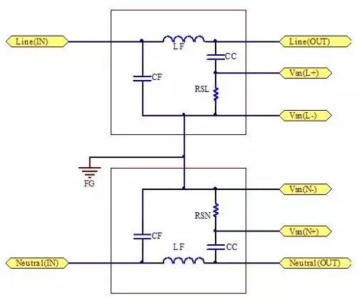
The internal circuit of the LISN (Linear Impedance Stabilization Network) is shown in Fig. 4. After the input power source enters the LISN from the left, the low-frequency noise of the power supply is filtered through the LF and CF, and is obtained by the coupling capacitor CC and the detection resistor RSL/RSN. The high-frequency signal Vsn, and then this signal through the receiver or spectrum analyzer to get the magnitude of its amplitude (dBuV).
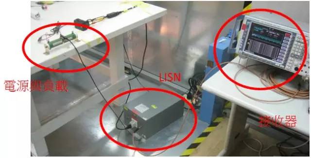
Please remember that the input wire should not be in contact with the ground. I once had experience with the input wire and the ground, and the experience of reading about 10dB difference. In addition, the power supply of the peripheral instruments needs to be clean and is isolated from the main power supply. Otherwise, it is very easy. Due to common ground and common mode interference, many test sites will directly use an extension cord to use an external power supply to give the surrounding, but this method may still be disturbed due to the common ground, if it can be connected to another LISN is a comparison In a good way, there are LF and CF in the LISN for signal isolation.
4 Countermeasures Basic concepts of EMI conduction
4.1 Differential Mode Signal and Common Mode Signal
Conduction measurement method shown in Figure 5, Figure 6, is measured by the receiver between the L / N / GND frequency and amplitude, and the signal exists between the L and N called differential mode signal, As shown in Fig. 5, the signal exists between L and FG or between N and FG. As shown in Fig. 6, it can be said that forming a loop with FG is called common mode signal.
The input source of the general power supply is taken from L and N, so in the electromagnetic interference design of the power supply, the suppression of the differential mode component is extremely important, especially the front frequency band 150K~1MHz is mostly the main frequency and frequency multiplication of the switching power supply. Differential mode interference.
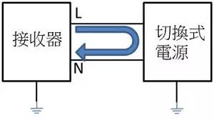
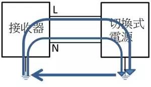
Fig. 7 shows the result of a conduction test before the countermeasure. The front end is the frequency doubled mode interference caused by the operating frequency of the IC plus the common mode interference of the body. The figure shows that the frequency between each peak is 100 KHz. It can be judged that the operating frequency of this IC is 100KHz, and the measured reading is linearly attenuated by the frequency multiplied by the IC 100KHz, so there is a differential mode interference signal caused by the IC operating frequency every 100KHz, and it can be said that In the pre-frequency band, the common-mode signal goes down in a linear plane, while the differential-mode signal is superimposed over the common-mode.
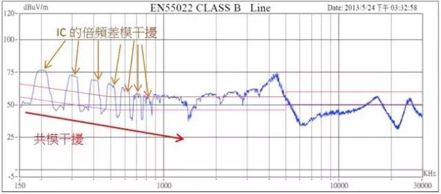
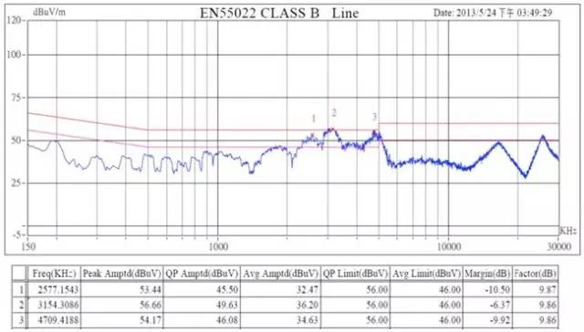
Fig. 8 shows the test results of the same machine after the countermeasures. After the countermeasures, the worst case is still more than 6dB, which has met most of the customer's requirements.
Generally, when testing, it is necessary to test L and N. Generally, the readings of L and N will not differ too much. If the difference is large, it is generally caused by a strong common mode energy of a certain item.
The input voltage to be tested is determined by the application's safety regulations. Generally, 110 V and 230 V are used for high and low voltage measurement. In addition, the product needs to be burned for a long time when confirming the conduction test, sometimes due to burning. Overheating of magnetic components results in abnormal inductance and worse EMI.
4.2 Electromagnetic Interference, Electric Field Interference and Magnetic Field Interference
Electromagnetic interference (EMI, Electrical Magnetic Interference) can be divided into two kinds of electric field interference and magnetic field interference, electric field and magnetic field are two different properties, but the energy between the two will affect each other, the electric field will change with time. Magnetic fields, and magnetic fields that change with time, also generate electric fields. These constantly oscillating electric and magnetic fields together form electromagnetic interference (electromagnetic waves).
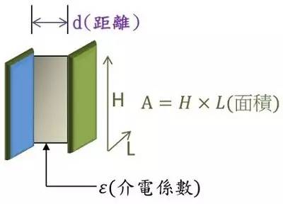
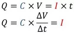
Generally for the electric field, we can use the following charge formula and capacitance formula to explain it.
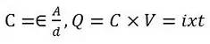
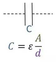
When the potential at both ends of the capacitor is at a voltage difference in time, a current is generated based on the charge formula (voltage/time change, as shown in Figure 12), as shown by the red arrow in Figure 11, and any current generated must be Returning to its own starting position via another path forms a current loop, as indicated by the brown dotted arrow, which causes electric field disturbances due to the current loop caused by voltage fluctuations.
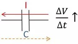
Therefore, the way to improve the electric field interference is to reduce the loop current. According to the above two formulas, we can reduce the coupling capacitance, such as reducing the area of ​​contact between two conductors/increasing the distance/change between them. The medium and other ways to reduce the capacitive effect, or reduce the voltage difference or time rate of change to reduce the electric field induction.
Rectangular I/O Connectors
Antenk offers an expansive product line of I/O connectors including USB, HDMI, D-Sub, Modular Jacks, SFP, QSFP+, CXP, iPass+, iPass+ HD and more. In addition to standard I/O connectors and matching cable assemblies.Except a comprehensive range of standard Input/Output connector solutions for high-speed electronic data communication, Antenk engineers can design customized solutions. This extensive selection of I/O connectors and matching cable assemblies includes numerous next-generation solutions.All of our I/O connectors feature a variety of orientation options, as well as PCB and cable mount offerings.
Antenk develop and specify high-performance I/O's throughout a wide variety of industries. These include SAS, SATA, PCIe, HSSG, FIBRE CHANNEL, INFINIBAND, IEC, CEA, IEEE, VESA, USB and many more.
I/O Connectors Application
Consumer / PC Products
Networking / Telecommunications Products
Mobile Products
Industrial Products
Antenk can deliver standard and custom options of the following I/O connectors:
1394 Connector
Centronic Connector
D-Sub Connector
DVI Connector
Display Port Connector
HDMI Connector
Half Pitch SCSI Connectors
USB Connector
V.35 Connector
OBD Connector
I/O Connectors General Specifications


ELECTRICAL CHARACTERISTICS
Contact Current Rating:5Amperes.
Dielectric Withstanding.
Dielectric Withstanding Voltage:AC 1000Vr.m.s.
Insulation Resistance:500 Megohms Minimum at DC500V.
Contact Resistance:25 Milliohms Maximum.
Operating Temperature:-55℃~105℃.
")
MATERIALS:
Contacts:Brass.
Insulator:PBT,UL94V-O Rated.
Shell:Cold Rolle Steel.
Metal Watertight Frame:PBT,UL94V-0.
O-Ring:Silicone.
NOTE:
Position:09PIN,15PIN,25PIN,37PIN.
Rectangular Connector,Rectangular I Connectors,Rectangular O Connectors,Male Connector Rectangular,I/O Connectors,Input/Output Connectors
ShenZhen Antenk Electronics Co,Ltd , https://www.antenkconn.com