
Resistance is almost an indispensable part of all circuits. Commonly, there are many resistors with different resistance values. However, in some circuits, different resistance values ​​are needed at the same position at different times. In some occasions where accuracy is not high, sliding rheostat Realized, but we can not determine the specific resistance. With the further development of technology, in order to meet the needs of teaching and research in certain occasions, resistance boxes with resistance values ​​determined and adjustable came into being. The principle that the resistance box provides the resistance value is the different resistance value obtained through the series and parallel connection of the resistance, so the number of resistors used is large, and the accuracy is not high enough, and it is necessary to select the corresponding gear for each digit of the required resistance , More troublesome and not intuitive enough. In some production applications (such as product verification), several sets of different resistances need to be provided at the same time, and they must be provided repeatedly (such as product aging detection experiments), which requires the resistance value to be recorded, which is not available in previous resistance boxes. With memory function, can not meet the requirements.
This article introduces the use of FPGA to realize the provision of control resistance, and the hardware is designed by software. Various software can be used for various simulations during the design process. At the same time, the entire system can be integrated on a chip, with small size, low power consumption, and reliability High, and because of its internal storage unit, it can meet the above "memory" function.
1 Hardware circuitThe hardware system of FPGA-based programmable resistance system (as shown in Figure 1) is mainly composed of the following functional modules:
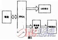
1.1 Main controller FPGA
The FPGA (Cyelone II series selected in this design) control center is the core of the entire design. The main control implements the processing of the system ’s keyboard input, and converts it into output data according to the input information, and controls the corresponding relay to pull in, thereby obtaining Different resistance.
In the past, the main controller of the programmable network was controlled by a digital circuit, or by a single-chip computer. This circuit was controlled by an FPGA. EPGA is a large-scale integrated circuit device that has appeared and been widely used in recent years. Its characteristics are directly facing users, with great flexibility and versatility, easy to use, fast hardware testing and implementation, high development efficiency, and low cost , Short time to market, simple technical maintenance, good work reliability, etc. Therefore, it is more flexible for designing programmable resistors.
At present, the companies that mainly produce FPGA products on the market include LatTIce, Xilinx, Altera. In the teaching process, generally use the FLEX series and Cyclone series produced by Altera. In view of the cost and versatility of the product, CycloneII is used in this experiment. It is the second generation of low-cost FPGA series. It has unique features: NiosII embedded processing
Support, embedded 18 * 18 digital signal processing multiplier, medium-capacity on-chip memory (can meet the requirements of this design) medium-speed I / O pins and memory interface. It is more suitable for this design in terms of cost performance, so this series is selected in this design.
1.2 Keyboard input circuit
The keyboard input circuit mainly realizes the setting of the output resistance value. The 4 * 4 simple keyboard input used in this design can meet the requirements. It can provide 16 keys with simple and clear numeric keys and function keys, including: numeric input keys: Numeric keys 0 ~ 9, press the numeric keys, enter a number, it can be displayed on the corresponding nixie tube.
Function keys: "Resistance 1", "Resistance 2" This design can provide two sets of resistance at the same time, you can choose resistance 1, can also choose resistance 2, provide a set of resistance, can also provide two sets of resistance .
"Storage": Press the storage key after entering a number, so as to be able to store several data, after operation, it will work according to the sequence of data storage and preset time to provide data cyclically.
"Run": This key is used as the start key after storing data.
"Stop": Stop providing resistance.
"Reset": It can be used to modify data. After pressing this key, all previously stored data can be cleared, and then a group of data can be reset.
1. 3 relay resistance network
Resistance network. The principle diagram is shown in Figure 2. From the figure, it can be seen that the closing of the switch determines whether the corresponding resistance is connected or not. In this design, the 8421 encoding principle is used to control the resistance.
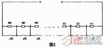
The resistance used in this design should be accurate to 0.1 Ω, so the resistors used in this resistor network are all precision resistors. Here we take the example of providing a resistance within 1500Ω. This resistance network is implemented in series. The 8421 coding method can be achieved by controlling the corresponding relay and shorting its corresponding precision resistor. Taking the internal resistance of 1500 Ω as an example, only 16 resistors can meet the requirements. By controlling the opening or closing of the relays J1 to J16, the corresponding resistance will be connected or disconnected, and the last connected resistance is added in series to get the output resistance value.
If a preset value is input through the keyboard, if the input value is 545.7Ω, the output resistance value can represent R = 400 + 100 + 40 + 4 + 1 + 0.4 + 0.2 + 0.1. That is, you only need to connect these resistors, the corresponding relays J1, J2, J3, J5, J7, J11, J13, J15 should be opened, and the rest of the relays should be closed. The corresponding binary code is (0101 0100 0101 0111) B. It can be seen from this column that with 16 resistors, the accuracy within 1500 Ω can be achieved. Any resistance of 1 Ω, using a small number of resistors, through the program to control the resistance access, the volume is smaller, at the same time, maintenance is also more convenient, if you need a resistance greater than 1500 Ω, you can also increase the resistance according to this principle (such as 8000 , 4000, 2000, 1000, etc.), because this design provides two resistors at the same time, it also needs 16 same resistors, the principle is the same as above. can).
1.4 Output display circuit
The main function of the output display circuit is to display in real time the size of the corresponding keyboard input resistance value, the number of current working steps and the preset time. According to the requirements, this experiment uses a digital tube to display its resistance value, which can meet the requirements. In order to display the above data, each resistance value display requires at least nine digital tubes, five of which are used to display the current resistance value. Two digits are used to display the current working steps, and two digits are used to display the working time of the data. If static display control is adopted, a considerable number of pin resources (9 & TImes; 2 & TImes; 8 = 144) will be required. The use of FPGA pin resources, the use of scanning in this design to achieve dynamic display of LED.
2 Software design and some simulation resultsIn this design, the main control program is implemented through FPGA software programming. Software design can be roughly divided into three large modules: keyboard scanning module, LED display module, relay resistance drive circuit module.
2. 1 keyboard scanning module
The keyboard scanning module is mainly used to detect the data input from the outside world, and is mainly composed of a frequency divider circuit, a keyboard scanning counter circuit, a keyboard row and column key detection circuit, a key jitter elimination circuit and a keyboard coding circuit.
Because the external frequency in this design is generally a 6MHz signal as the clock signal, but keyboard scanning does not require such a high frequency, so a frequency divider circuit is needed to reduce its frequency to 1kHz. The keyboard scan counter mainly serves the keyboard row and column key detection circuit and keyboard coding circuit. The keyboard row and column key detection circuit is used to detect the position of the row and column where the keyboard input is located. The effect causes the button enable bit to generate unnecessary jitter changes, resulting in the result of repeatedly counting the number of button presses. At the same time, the code of the keyboard position is not the key value on the keyboard, so the keyboard coding circuit should be used to transfer the real key value.
2. 2 LED display module
The LED display module uses a dynamic display method. This implementation method is to turn on each LED digital tube in turn and display it in a loop. It is very important to control the delay between the digital tubes in this display mode. According to the principle of persistence of human vision, LED If the digital tube is turned on more than 16 times per second, the human eye cannot tell that the LED digital tube is not bright for a short time. It is considered to be always on, but the delay is not as small as possible, because the LED digital tube needs to reach a certain brightness. time. In order to achieve better results, the delay in this design is 0.005s.
2. 3 relay resistance drive circuit module
The relay resistance driving circuit module is mainly based on the FPGA to determine whether some of the corresponding resistance should be connected according to the resistance value input by the keyboard, so that the relay corresponding to the resistance is closed or opened, and the corresponding signal 1 or O can be given.
2.4 Simulation results
It can be seen from the above theory that the generating principle of the resistance 1 and the generating principle of the resistance 2 are exactly the same. In order to make the simulation result more clear, the simulation waveform here only uses the resistance 1 to verify its correctness. The simulation waveform is shown in FIG. 3.
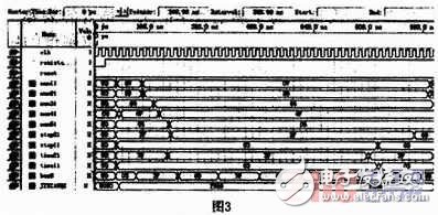
This figure is a part of the simulation diagram, only a few representative signals are selected for display and explanation. It can be seen from the figure that there are clock signal clk, reset signal reset, resistance 1 selection signal resistancel, numll to num51. They are the decimal place, unit place, tens place, hundred place, dry place of resistance value. Step11 and step21 show the ones and tens of the current working step respectively, and TIme11 and time21 show the ones and tens of the working time respectively. Bus9 is a data signal during dynamic display, and JIDIANQI represents the switching state of 16 relays. It can be seen from the figure above that the segment code of the decimal place of the resistor is 07H, the corresponding binary is 00000111, and the corresponding displayed number is 7 that is the decimal place is 7. Similarly, we can see that its single digit is 5, ten digits Is 4, the hundreds digit is 3, and the thousands digit is 1, so the resistance is 13345. 7Ω, it can be seen from the figure that the bus is cyclically transmitting time, step and value information. According to the resistance, its The corresponding relay will be closed. According to the above resistance network principle, J4, J6, J8, J9, J10, J12, J14 are closed, and the rest of the relays are open, that is, the corresponding binary code is (0010101110101000) B, converted to hex The system is 2BA8, and it can be seen from the above figure that the verification result is correct.
3 ConclusionThe system realizes this module through the introduction of FPGA to provide resistance, and also integrates other surrounding digital logic circuits into the chip. This not only solves the particularity of the system, but also enhances the anti-interference of the system, improves the control accuracy, and simplifies debugging. In addition, the system also implements hardware such as drive circuits and codec circuits in the FPGA chip through VHDL language. Compared with the previous analog circuit and single-chip implementation methods, fewer components are used and the volume is smaller. , It is more convenient to modify. Has a very good market prospect.
Imported Stainless Steel Wire,Stainless Steel Straight Wire,Soft Reinforcement Stainless Steel Binding Wire,Bright Surface Stainless Steel Wire
ShenZhen Haofa Metal Precision Parts Technology Co., Ltd. , https://www.haofametals.com