
The figure below is the clock tree of the STM32. From the tree we can see that the STM32 clock has two sources - the internal clock and the external clock. According to the clock frequency, it is divided into a high-speed clock and a low-speed clock. Therefore, the STM32 clock has four sources—a high-speed external clock signal (HSE), a low-speed external clock signal (LSE), a high-speed internal clock signal (HSI), and a low-speed internal clock signal (LSI). ~4 annotation. 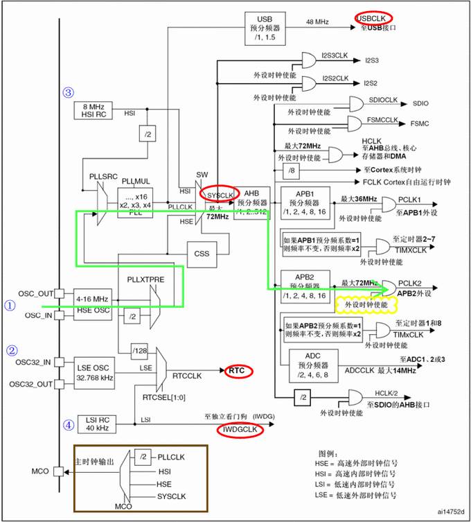
1HSE high-speed external clock: provided by an external 4~16MHz crystal or active crystal oscillator, usually 8MHz, and 8MHz on the ST 3-in-1 board.
2 LSI low-speed external clock: external crystal supply, mainly to the real-time clock (RTC), typically 32.768kHz.
3HSI High Speed ​​Internal Clock: 8MHz clock generated by the internal RC oscillator, but not stable enough.
4 LSI low-speed internal clock: The clock supplied to the RTC generated by the internal RC oscillator, with a frequency between 30 kHz and 60 kHz, usually about 40 kHz.
The clock is finally supplied to the STM32 with four large blocks, which are circled with a red ellipse - the USB 48MHz clock, the system clock SYSCLK, the real-time clock module RTC, and the independent watchdog clock IWDGCLK. The most important and largest head is the system clock SYSCLK, which can be directly connected to the internal or external high-speed clock, or the internal and external high-speed clocks are provided after the PLL multiplier, and the system clock is separately supplied to the Cortex core, SDIO, AHB bus, DMA, APB1, APB2, etc.
We usually use an external 8MHz high-speed clock (HSE), so we focus on HSE. Let's take the clock on the previous GPIO as an example. According to ST's Datasheet, GPIO is on the APB2 high-speed peripheral bus. The green line in the figure is the clock flow. Let's look at it step by step.
After the 8MHz external crystal (or crystal oscillator) is input, it passes through a switch PLLXTPRE (HSE divider for PLL entry). This switch determines to divide the HSE by 2 and input it to the PLL or directly to the PLL. We choose not to divide.
The clock then goes to the second switch, PLLSRC (PLL entry clock source), which determines the clock source of the PLL, whether it is the internal high-speed clock divide-by-two clock or the PLLXTPRE output. We chose the latter, when the clock is still 8MHz before entering the PLL, because we have no crossover at PLLXTPRE.
When the PLL multiplier is reached, the number of multiplier systems is determined by PLLMUL. You can select 2~16 multiplier output, but remember that the PLL output frequency is up to 72MHz, so we choose 9x, so the PLL output is the highest 72MHz PLLCLK clock. . At this time, PLLCLK provides a clock for the USB.
The switch SW determines the clock source of SYSCLK. As mentioned above, we use PLLCLK as the source of SYSCLK, so the system clock SYSCLK is 72MHz.
Before the peripherals are supplied, we pass the AHB prescaler. We choose not to divide the frequency. Before the GPIO is supplied, we must pass the APB2 prescaler. Because APB2 is a high-speed peripheral, we choose not to divide the frequency, so GPIO The clock is 72MHz. Note that the maximum frequency of the low-speed peripheral APB1 is 36MHz, so when using the peripherals of the APB1, pay attention to setting up the crossover system. Also note that to use peripherals, first enable the peripheral clock, as shown in the yellow cloud box. This is because the STM32 uses a low-power design, and the clock is not enabled for unused peripherals to reduce power consumption.
How is the clock setting implemented in the program? Here we use the previous GPIO program to analyze step by step. Of course, the previous program is based on the ST library, in fact, is to analyze the official library of ST.
We see that the first line of code in the main() function is calling a function:
SystemInit();
This function is in system_stm32f10x.c:
Void SystemInit (void)
{
/* Reset the RCC clock configuration to the default reset state(for debug purpose) */
/* Set HSION bit */
RCC->CR |= (uint32_t)0x00000001;
/* Reset SW, HPRE, PPRE1, PPRE2, ADCPRE and MCO bits */
#ifndef STM32F10X_CL
RCC->CFGR &= (uint32_t)0xF8FF0000;
#else
RCC->CFGR &= (uint32_t)0xF0FF0000;
#endif /* STM32F10X_CL */
/* Reset HSEON, CSSON and PLLON bits */
RCC->CR &= (uint32_t)0xFEF6FFFF;
/* Reset HSEBYP bit */
RCC->CR &= (uint32_t)0xFFFBFFFF;
/* Reset PLLSRC, PLLXTPRE, PLLMUL and USBPRE/OTGFSPRE bits */
RCC->CFGR &= (uint32_t)0xFF80FFFF;
#ifdef STM32F10X_CL
/* Reset PLL2ON and PLL3ON bits */
RCC->CR &= (uint32_t)0xEBFFFFFF;
/* Disable all interrupts and clear pending bits */
RCC->CIR = 0x00FF0000;
/* Reset CFGR2 register */
RCC->CFGR2 = 0x00000000;
#elif defined (STM32F10X_LD_VL) ||defined (STM32F10X_MD_VL) || (defined STM32F10X_HD_VL)
/* Disable all interrupts and clear pending bits */
RCC->CIR = 0x009F0000;
/* Reset CFGR2 register */
RCC->CFGR2 = 0x00000000;
#else
/* Disable all interrupts and clear pending bits */
RCC->CIR = 0x009F0000;
#endif /* STM32F10X_CL */
#ifdefined(STM32F10X_HD) || (defined STM32F10X_XL) || (defined STM32F10X_HD_VL)
#ifdef DATA_IN_ExtSRAM
SystemInit_ExtMemCtl();
#endif /* DATA_IN_ExtSRAM */
#endif
/* Configure the System clock frequency, HCLK, PCLK2 and PCLK1 prescalers */
/* Configure the Flash Latency cycles and enable prefetch buffer */
SetSysClock();
#ifdef VECT_TAB_SRAM
SCB->VTOR = SRAM_BASE | VECT_TAB_OFFSET; /* Vector Table Relocation in Internal SRAM. */
#else
SCB->VTOR = FLASH_BASE | VECT_TAB_OFFSET; /* Vector Table Relocation in Internal FLASH. */
#endif
}
We can see that the system is in front of a system Reset or Disable, and finally called (red mark)
SetSysClock();
The SetSysClock() function is also located in the system_stm32f10x.c source file:
Static void SetSysClock(void)
{
#ifdef SYSCLK_FREQ_HSE
SetSysClockToHSE();
#elifdefined SYSCLK_FREQ_24MHz
SetSysClockTo24();
#elifdefined SYSCLK_FREQ_36MHz
SetSysClockTo36();
#elifdefined SYSCLK_FREQ_48MHz
SetSysClockTo48();
#elifdefined SYSCLK_FREQ_56MHz
SetSysClockTo56();
#elifdefined SYSCLK_FREQ_72MHz
SetSysClockTo72();
#endif
/* If none of the define above is enabled, the HSI is used as System clock
Source (default after reset) */
}
Since we are using a 72MHz clock, we definitely define the macro SYSCLK_FREQ_72MHz, so we call the function SetSysClockTo72(). We continue to track and we will find that at the beginning of the source file, we have determined:
#define SYSCLK_FREQ_72MHz 72000000
Set 72MHz in detail in the SetSysClockTo72() function, and do not analyze it step by step.
As mentioned above, when using peripherals, the corresponding peripheral clock should be enabled. For example, when using the GPIOB for the pipeline experiment, the following library function is called in the program to set the peripheral clock:
RCC_APB2PeriphClockCmd( RCC_APB2Periph_GPIOB, ENABLE);
In addition, the STM32 can also output the clock, as shown in the bottom left corner of the brown box, which can be determined by the MCO. The PLL clock divides by two or HIS or HSE or the system clock as the main clock output.
Modify Sine Wave Inverter,Mini Modified Wave Car Inverter,Modify Sine Wave Power Inverter,Modified Sine Wave Inverter With Rohs
GuangZhou HanFong New Energy Technology Co. , Ltd. , https://www.gzinverter.com