Everyone is familiar with laser processing. CO2 laser, fiber laser and semiconductor laser are the mainstream lasers in industrial applications, in the subtle and nanosecond order, but in the past decade, ultrashort pulse laser finishing technology has made rapid progress. In the femtosecond and picosecond scales, that is, the laser micromachining we are going to say today!
Laser micromachining
People have tried laser micromachining very early. However, due to the long pulse width and low laser intensity of the laser, the material melts and continues to evaporate. Although the laser beam can be focused into a small spot, the thermal shock to the material is still large, which limits the precision of the processing. Only by reducing the thermal impact can the processing quality be improved. When the laser is applied to the material in a pulse time of the order of picoseconds, the processing effect changes significantly. As the pulse energy rises sharply, the high power density is sufficient to strip the outer electrons. Since the laser interacts with the material for a short period of time, the ions are ablated from the surface of the material before it is transferred to the surrounding material, and do not have a thermal effect on the surrounding material. Therefore, it is also called "cold processing". . With the advantages of cold working, short and ultrashort pulse lasers enter industrial production applications.
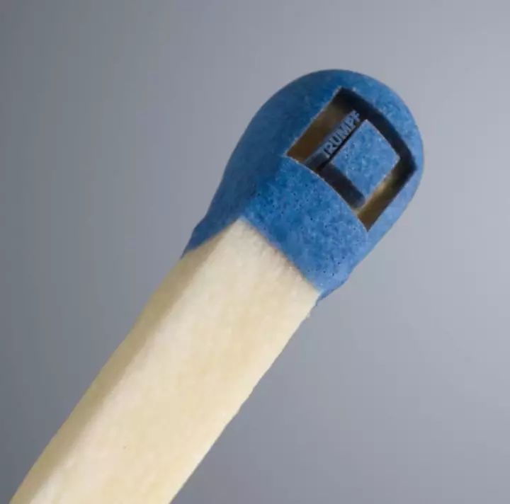
Figure 1 Ultrashort pulse cold processing ablation process on the match head
How fast is it?
The pulse width produced by short pulse lasers is defined on the order of picoseconds and femtoseconds. 1 picosecond is equal to 10-12 seconds, 1 femtosecond is equal to 10-15 seconds. Maybe more abstract, but we can convert it into a form of distance to compare. For example, the speed of light is 3x10⁻⁸ meters per second. The time it takes for light to travel from Earth to the Moon is about 1.3 seconds, while the distance of light movement in a picosecond is 0.3 mm!

What can you do with super fast?
The rapid development of short-pulse laser technology has made it widely used in the industrial range, and new applications are found almost every day. At present, short pulses are mainly concentrated in the following application fields.
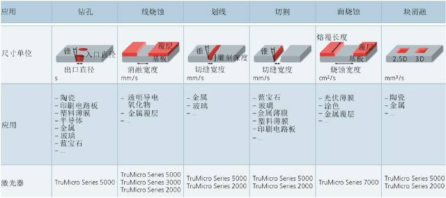
Figure 2 Classification of laser micromachining
1 drilling
In circuit board design, ceramic substrates have been used to replace conventional plastic substrates for better thermal conductivity. In order to connect electronic components, it is generally necessary to drill up to hundreds of thousands of small holes of 40100 μm in diameter. It is therefore important to ensure that the stability of the substrate is not affected by the heat input during the drilling process. The picosecond laser is the ideal tool for this application. The picosecond laser can complete the hole machining in the form of impact drilling and ensure the uniformity of the hole. In addition to the board, picosecond lasers can be used for high quality drilling of plastic films, semiconductors, metal films and sapphire.
Printed circuit board micro-hole laser processing (picosecond level)
2 scribing, cutting
Lines can be formed by superimposing laser pulses by scanning. It is usually possible to penetrate deep into the ceramic through a large number of scans until the depth of the line reaches 1/6 of the thickness of the material. A single module is then separated from the ceramic substrate along these score lines. This separation method is called scribing. Another separation method is the use of ultrashort pulse laser ablation cuts, also known as ablation cuts. The laser ablate the material and removes the material until it is cut through. The benefit of this technique is the greater flexibility in the shape and size of the machined holes. All process steps can be done with a picosecond laser.
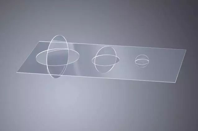
Figure 3 Zero slit cutting on transparent material
3-line ablation (removal of plating)
Another application that is often considered micromachining is the precise removal of the coating without damaging or slightly damaging the substrate material. The ablation can be either a few micrometers wide or a large area of ​​a few square centimeters. Since the thickness of the coating is usually much smaller than the width of the ablation, the heat cannot be conducted on the side. Therefore, a laser with a nanosecond pulse width can be used. High average power lasers, square or rectangular conducting fibers, flat top light intensity distribution, and the combination of these technologies make laser surface ablation available in the industrial field. For example: use Trump's TruMicro 7060 laser to remove the coating on the thin-film solar cell glass. The same laser can also be used in the automotive industry to remove corrosion-resistant coatings in preparation for subsequent welding.
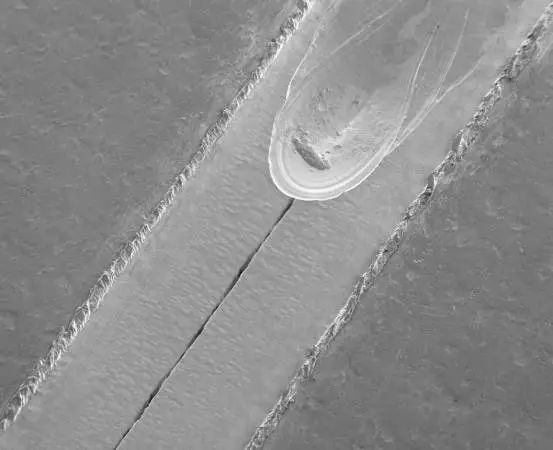
Figure 4 Removing the anti-corrosion coating
4 surface structuring
Structure can change the physical properties of the surface of the material. According to the lotus effect, the hydrophobic surface structure allows water to flow away from the surface. This feature can be achieved by creating a submicron structure on the surface with an ultrashort pulse laser, and the structure to be created can be precisely controlled by changing the laser parameters. The opposite effect, such as a hydrophilic surface, can also be achieved, and micromachining can also create larger sized structures. These processes can be used in fuel tanks in engines to create some wear-reducing microstructures, or structurally metal surfaces to weld to plastics.
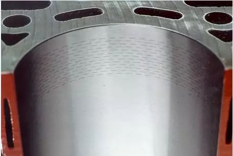
Figure 5 Short pulse for surface structuring
5 engraving
Engraving is the creation of three-dimensional shapes by ablating materials. Although the size of the ablation may exceed the scope of micromachining in the traditional sense, the accuracy required is such that it is classified into such laser applications. Picosecond lasers can be used to machine the edge of polycrystalline diamond tools in milling machines. Laser is the ideal tool for processing polycrystalline diamond, which is an extremely hard material that can be used to make milling cutter edges. The engraving technique is used to machine the chip flutes and teeth of the milling cutter. In this case, the benefits of the laser are non-contact and high machining accuracy.
Picosecond laser processing technology for machining bits with superhard materials (picosecond)
In short, micromachining has a very broad application prospect, and more and more daily necessities are entering our field of vision through laser micromachining.
Electric Meters Battery Crp2,Crp2 Lithium Battery,Car Gps Battery,Monitoring Primary Battery 6V
Jiangmen Hongli Energy Co.ltd , https://www.honglienergy.com
