A Class A amplifier with dynamic bias [Circuit principle]
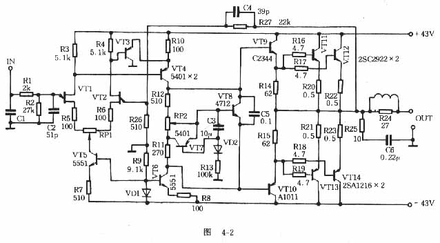
As shown in Figure 4-2, the input stage of this power amplifier is a pair of field effect transistors, which has the advantages of high input impedance, large dynamic range and low noise. VT3 and VT4 form the second stage of amplification. VT5 provides 1.8mA of current to VT1 and VT2; VT6 provides a constant current of 9.5mA to VT3 and VT4. Due to the conduction of VD1, even if the current voltage fluctuates, it will not affect the reference voltage of VT5 and VT6, which ensures the stability of the current of VT1 and VT2. VT9 ~ VT14 form a complementary output stage, and its output current is controlled by VT8. VT8 is a constant voltage circuit, the dynamic internal resistance is small, the voltage of Vce8 is constant, and the static working current can be adjusted by adjusting RP2. VT7, C3, R13, and VD2 form a dynamic bias circuit. Its principle is: when the signal input increases, VT7 lowers the base current of VT8, Vce of VT8 increases, and the current of VT9 ~ VT14 also increases , The highest peak value can reach 4 ~ 5A, so that the push-pull output automatically works in the Class A state, not only reduces crossover distortion and harmonic distortion, but also improves the power supply utilization rate, the dynamic bias control amount is determined by Rl3. C5 is a large-loop negative feedback capacitor for accelerating high-frequency signals, and has a phase leading compensation effect. Can reduce transient distortion and intermodulation distortion, and can prevent self-excitation. The input stage is also added with a high-frequency filter network to filter out unnecessary high-frequency noise and improve the signal-to-noise ratio. 
ã€Component selection】
The BVceo of the transistor used in the circuit is required to be greater than or equal to twice the power supply voltage. Field effect tube VDS> / = 50V, Gm must also be consistent. The complementary output stage should measure the DC magnification from small current to large current. It requires good linearity, and the difference between each bit does not exceed 1%. The input stage's? T can be selected higher, and the output stage's? T should be lower. The resistor should be a metal film resistor with stable performance. C3 selects CA series, and the rest are CBB capacitors. In the selection of tubes, attention must be paid to the selection of the transistors in the driving stage. In fact, the working state of the push level determines whether the output work of the unlevel can be relaxed. The power supply voltages used in today's high-power amplifiers are relatively high, the output tube drive current is also relatively large, and the power consumption of the driving stage is considerable. This is why the driving stage of the advanced power amplifier chooses medium power and high power tube wells and radiators.
ã€Installation and commissioning]
Because all levels of the circuit are directly coupled. Failure of one of the components may affect the working state or even damage the transistor. Therefore, the quality of components must be carefully checked. During installation, the two potentiometers that adjust the zero potential and quiescent current can be installed near VT1, VT2, and VT7. The housing must be well grounded. The high-power tube and the emitter resistor are installed on a radiator with a large enough area to avoid Unnecessary parasitic coupling occurs through the large current through the circuit board. VT8 is installed in the middle of the four transistors for temperature compensation to stabilize the static operating current.
The commissioning of this amplifier is very simple. First, connect a 40-60W, 27ohm or 36V machine tool working light bulb with a power of 60W as a dummy load to the unterminated amplifier. The midpoint voltage measured with a multimeter should be about 0V. If the requirements are not met, it may be that the differential tubes are not paired, or the component pins are soldered incorrectly. Debugging of quiescent current: adjust RP2 so that the voltage drop across the emitter resistance of the output tube is about 100mV, and the quiescent current is at 200mA. |


![[Photo] 60W Class D amplifier composed of STA500](http://i.bosscdn.com/blog/20/06/41/7211954437.jpg)
![[Photo] A schematic diagram of an ultra-low power regulator circuit](http://i.bosscdn.com/blog/20/06/41/623956167.jpg)
![[Photo] A high-precision constant temperature controller circuit without temperature step zone](http://i.bosscdn.com/blog/20/06/41/6172140890.gif)
![[Photo] One provides ± 15V and ± ...](http://i.bosscdn.com/blog/20/06/41/5232314954.gif)

![[Photo] A walkie talkie circuit](http://i.bosscdn.com/blog/20/06/41/5205822650.gif)


![[Photo] 60W Class D amplifier composed of STA500](http://i.bosscdn.com/blog/20/06/41/7211954437.jpg)
![[Photo] A schematic diagram of an ultra-low power regulator circuit](http://i.bosscdn.com/blog/20/06/41/623956167.jpg)
![[Photo] A high-precision constant temperature controller circuit without temperature step zone](http://i.bosscdn.com/blog/20/06/41/6172140890.gif)
![[Photo] One provides ± 15V and ± ...](http://i.bosscdn.com/blog/20/06/41/5232314954.gif)

![[Photo] A walkie talkie circuit](http://i.bosscdn.com/blog/20/06/41/5205822650.gif)