
As one of the basic dimensions of physics, time is an important reference indicator for system operation, and IRIG-B code is an international standard time code. Its performance is superior, its implementation and use method are simple and easy, and it is very suitable for high-precision time transmission. In the system.
FGPA has the characteristics of convenient programming, high integration, fast speed, etc. It can be repeatedly programmed, erased and used, and can realize different functional requirements without changing the hardware design. Using FPGA to realize timing and frequency division, generating time signals and various synchronization signals can make the time interface module more integrated and more maintainable.
In this paper, a high-speed time unified system design scheme based on FPGA is proposed in combination with the actual time system project. It is based on Altera [1] Cyclone series FPGA [2-3] chip, using schematic and Verilog language programming [4]. . By receiving external references such as GPS, Beidou, and B code, and selecting one of them to generate the IRIG-B code signal and each pulse signal synchronized with it, it can be used by other subsystems.
1 overall system design
The system hardware includes the time card (installed on the server) and the IRIG-B code terminal [6]. Figure 1 shows the composition of the system equipment.
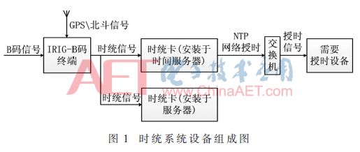
The IRIG-B code terminal can realize the dual system time signal redundant reception of the GPS satellite system and the Beidou satellite system and the direct reception of the external B code signal, and generate multiple DC or AC IRIG-B codes to be sent to the time card.
The time card receives the IRIG-B code directly and automatically obtains the standard time information through the decoding circuit, and sends the time information to the server with the time card through the VPX bus. After receiving the time information, the server sends the information to the server itself and the workstations in the network. The terminal performs network timing to realize strict monitoring and output of the device's own signal to improve the reliability of the system and meet the time synchronization requirements.
2 IRIG-B code coding principle
IRIG-B code is a commonly used serial transmission time format code. Compared with parallel transmission mode, it has simple physical connection, large amount of information, high resolution, long transmission distance, strong anti-interference ability and standardization. interface. According to the different requirements of time precision and the transmission distance of B code, the B code adopts two types of codes: B (DC) DC code and B (AC) AC code. Each symbol of the B(DC) code is a pulse signal, which can achieve higher precision time synchronization, but the pulse signal is rich in spectrum, the narrowband channel cannot be transmitted, and is suitable for short-distance cable transmission; the B(AC) code can be used. Standard voice bandwidth (0.3 kHz to 3.4 kHz) channel transmission, the transmission distance is farther, but the transmission accuracy has a certain loss. The B(AC) code can be obtained by amplitude modulating a standard sine wave carrier from a B (DC) code. Different pattern transmissions can be selected according to different requirements. In this system, both patterns are applied.
3 B code terminal
The B code terminal can receive the GPS/Beidou timing signal and the alien B code signal, and generate a 1PPS pulse signal and a DC/AC time code signal through the codec process for use by the time synchronization device.
3.1 Principle and composition of B code terminal system
The schematic diagram of the B code terminal system is shown in Figure 2.
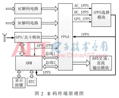
The B code terminal can simultaneously receive the GPS/Beidou signal and the alien B code signal. When the GPS/Beidou signal arrives, the GPS/Beidou module receives the timing signal through the antenna, sends the 1PPS pulse signal to the ARM and the FPGA, and simultaneously transmits the time information to the ARM in a serial manner; the ARM passes the solved time information and the valid flag through The custom bus and communication protocol are sent to the FPGA; after receiving the 1PPS and time information, the FPGA selects the time information or the self-defense mode according to the validity of the information, and generates a multi-channel AC/DC code and a 1PPS signal to output to the outside. . When the external B code arrives, the external B code signal is shaped and operated by the AC/DC decoding circuit, and then transmitted to the FPGA for encoding and decoding.
3.2 B code terminal unit module design
(1) GPS / Beidou module
The GPS/Beidou module with accuracy of 30 ns and 1 PPS is selected to transmit time signals to FPGA and ARM, and supports configuration of the chip through serial port commands.
The GPS/Beidou module output contains UTC year, month, day, hour, minute, and second. The ARM processor receives the whole second signal through the 1PPS interrupt provided by the module, and acquires the time information through asynchronous serial communication.
(2) External B code decoding circuit
When an external B code signal is used as a reference for generating an IRIG-B code, the external B code reference needs to be subjected to reception demodulation to generate reference seconds and serial time data. In this design, the demodulation of the external B code reference is performed using a hardware circuit.
(3) 1PPS selection module
The FPGA processes the GPS/Beidou signal and the alien B code signal to generate AC_1PPS, DC_1PPS, GPS_1PPS signals, which serves as the communication standard between ARM and FPGA.
(4) FPGA functional module design
As the core of the B code terminal, FPGA implements functions such as time code generation, synchronous frequency division, and external B code signal decoding. It mainly includes B (AC/DC) code generation module, B (DC) code decoding module, and B (AC). Code decoding module, etc. The working principle of each module is shown in Figure 3.
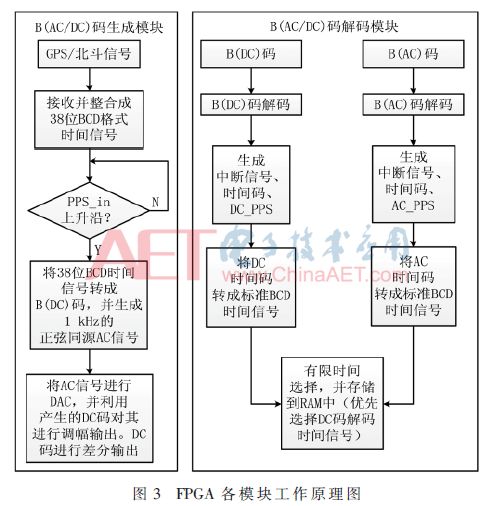
B (AC) code generation module: The FPGA generates an AC code according to the time information of the GPS/Beidou module, and the AC code of each bit of the high and low levels actually outputs a sinusoidal waveform corresponding to one cycle in the ROM, and the waveform control word sent by the FPGA is sent. To the DAC, the DAC output corresponds to the current value, and the sinusoidal waveform corresponding to the AC code high and low level is generated after being converted by the operational amplifier circuit, and finally the waveform is output through the 1:1 transformer.
B (DC) code generation module: The FPGA directly generates the TTL output of the DC code according to the time information of the GPS/Beidou module, and outputs the DC code output to the multi-channel DC code after single-ended/differential conversion.
B code decoding module: FPGA completes the decoding of the external B code to achieve accurate time information extraction and output.
4 hour card
The time card design adopts the universal VPX interface, which can receive the IRIG-B (DC) code and IRIG-B (AC) code input of the standardized time system. The device can capture the current time from the VPX bus [5-6] through the upper layer driver. Information, collecting interrupt signals of different frequencies. According to the specific requirements of the time card, the time card is divided into two main parts: hardware circuit design, IRIG-B code decoding, time acquisition software design.
4.1 Hardware Circuit Design
The overall system hardware includes the B code receiving circuit, the VPX interface circuit, the B code decoding circuit and the power supply circuit. The specific hardware structure design block diagram is shown in Figure 4.
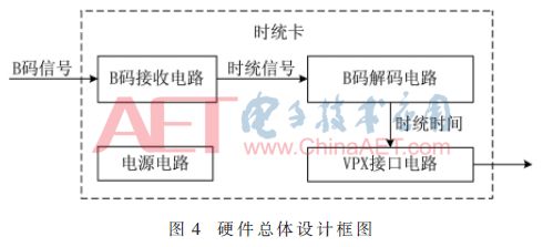
The B code receiving circuit comprises two parts, namely, the receiving of the B (AC) code and the B (DC) code. After the receiving circuit, the final two patterns are transmitted to the B code decoding circuit in a TTL level manner.
The B code decoding circuit is mainly composed of an FPGA chip and a peripheral circuit, and the decoding of the B code is completed through FPGA programming to realize the extraction of time information.
4.2 FPGA
The FPGA completes the decoding of the B code to achieve accurate time information extraction and communicates with the VPX interface.
The internal design block diagram of the FPGA is shown in Figure 5.
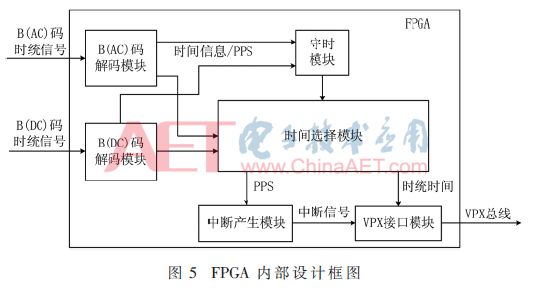
The B code decoding module of the FPGA mainly includes: a B (DC) code decoding module, a B (AC) code decoding module, a time selection module, an interrupt generation module, and a VPX interface module. The FPGA program can complete the extraction of time information, automatic switching of B (DC) code and B (AC) code, and can also realize the interrupt signal of different time by the PPS second pulse generated by the B code decoding process. The VPX interface program completes the reception of time information and interrupt signals and transmits them to the VPX bus.
The B(AC) code decoding module and the B (DC) decoding module respectively extract time information according to the code characteristics of the B code, and output valid time information, time valid flag and PPS second pulse.
The valid time selection module selects an output valid time signal according to the time valid signal of the B (AC) and B (DC) code decoding output, where the B (DC) code time information is preferentially selected.
The interrupt generation module generates accurate and different cycle interrupt time signals according to the PPS second pulse to provide a higher resolution time signal for the host computer.
The punctuality module is an update of the second pulse and time generated by the internal clock count of the FPGA when there is no B code input. The B code decoding module outputs a corresponding signal when the time information is not successfully decoded, and completes the switching of the punctual time by the time selection module. The punctual module automatically updates the time every second period when there is a B code input, and performs time counting by itself to complete the punctual function.
5 Experimental results
The B code terminal is connected with the time card, and under the condition of accessing the GPS/Beidou signal, the signal output by the host computer is used to read the signal output by the time card. In the reading process, in order to display the intuitiveness and simplicity, the information is printed only once at the initial time per second. In addition, in order to more accurately reflect the delay of the system and the upper computer reading, the upper computer test software adds the maximum and minimum delay of each interrupt when reading per second. Figure 6 shows the experimental results of the system operation.
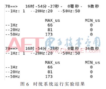
After many long tests, the maximum delay of each interrupt meets the design requirements.
6 Conclusion
The time system of this paper has simple peripheral hardware circuit and high reliability. The time system card uses VPX bus to communicate, which meets the performance requirements of high performance, high bandwidth and harsh environment of the shooting range computing platform. It has great development and application prospects. Successfully applied to a device. After a long period of work inspection, the equipment is stable and the indicators meet the requirements.
8 Inch Coaxial Speaker,Professional Coaxial Speaker,Ferrite Coaxial Speaker,Pro Audio Coaxial
Guangzhou BMY Electronic Limited company , https://www.bmy-speakers.com