
Abstract: This paper introduces an FPGA-based multi-channel signal acquisition circuit. The circuit uses the FPGA chip XC3S400 as the main controller of the circuit, and uses the electronic switch ADG708 to cyclically acquire 7 signals. The AD7667 is used as an analog-to-digital converter, which is controlled by the main controller FPGA to convert the collected analog signals into digital signals. signal. Then, through the single-chip microcomputer CY7C68013 to communicate with the host computer, the collected signal is read out by the host computer software and drawn. The effectiveness of the function of the acquisition circuit has been verified by experiments.
0 PrefaceData acquisition is a very important part of the signal processing process. The field programmable gate array FPGA has the characteristics of high integration, high efficiency, flexible design and low power consumption. The FPGA has its unique complex hardware logic control capability and real-time performance. Synchronization is widely used in data acquisition and storage systems [1 - 2]. This design proposes a design method of multi-channel data acquisition circuit based on FPGA. It is mainly used to obtain various flight parameters of the aircraft during flight, for the original data to be recovered after landing, to read the original flight data in the PC through the PC software and to realize the splitting and drawing of the original data for testing. Data analysis to evaluate and validate the performance of the aircraft.
1 hardware circuit design 1. 1 hardware circuit function The circuit completes the acquisition function of the recorder, and collects one DC voltage signal and six vibration sensor signals. The specific indicators are as follows:
(1) DC voltage: Measurement range: 0 to 100V; Accuracy: 1%; Sampling rate: 50kHz.
(2) Vibration sensor signal: Measurement range: ± 10g; Accuracy: 1%; Sampling rate: 10kHz.
In addition, the circuit completes communication with the host computer and controls the working state of the entire recorder. The various commands are sent to the recorder through the supporting PC software, and the digital signals stored in the flash are uploaded to the host computer for analysis.
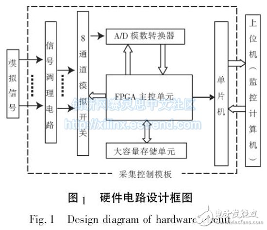
1. 2 principle of hardware circuitThe circuit working block diagram is shown in Figure 1. After the analog signal to be acquired is followed by the pre-conditioning circuit, the main controller FPGA controls the analog switch switching channel to realize the cyclic acquisition of the 6-channel sensor vibration analog and 1 DC voltage. The FPGA controls the analog-to-digital converter AD7667 to convert the acquired analog signal into a digital signal and write it to the flash memory. After the test, pass USB2. 0 The interface is connected to the upper computer, and the host computer software sends a reading command to the single-chip microcomputer to read the data in the flash memory to the upper computer for display and process analysis. The dotted line in Figure 1 is a multi-channel acquisition control module.
For a complex system, its functions are diversified, and hardware design is generally required to adopt a functional modular design method. A system is decomposed into multiple modules according to its functions. Each module has relative independence, and there is a certain relationship between local ranges, which is helpful for system design, debugging and maintenance, and easy to expand functions [3]. In the circuit design process, the main function modules are the acquisition recording function module and the USB interface module. Among them, the acquisition and recording module is the core of the whole circuit, the main task is to collect the signal to be tested, upload data and control other circuits.
2. 1 acquisition record module2. 1. 1 Acquisition module design The acquisition and recording module mainly completes the sampling, framing and recording of two three-axis vibration sensors (6 channels in total) and one DC voltage signal. The block diagram is shown in Figure 2.
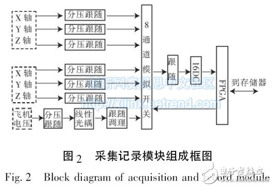
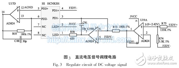
The DC voltage signal is measured from 0 to 100V. It needs to be divided before following. The voltage of the input chip AD824 is controlled to 0~3V, and is electrically isolated by the linear optocoupler HCNR201. Finally, the voltage range is adjusted to the analog switch ADG708. The input voltage range is 0 to 5V. The conditioning circuit is shown in Figure 3.
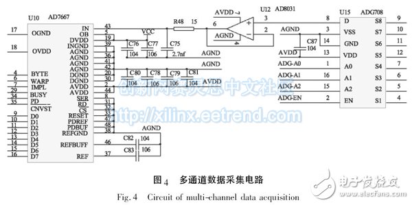
After the 6-channel sensor signal enters the circuit, the signal following the conditioning output of the amplifier AD824 enters the analog electronic switch ADG708 along with the conditioned DC signal. The ADG708 is controlled by the FPGA. The A0, A1, A2 address lines determine the signal output, and the output signal is output. The AD8031 was followed by an additional drive capability that was sampled by the AD7667. The sample word length is 16 bits, and the data after the acquisition of the frame is stored in the flash memory. The acquisition circuit design is shown in Figure 4.
2. 1. 2 AD7667 module
The AD7667 is easily driven. In this circuit design, the AD8031 is used as a driver to enhance the signal driving capability. The output signal is sent to the AD7667 for conversion. The resistance values ​​of R48 and C75 are recommended by AD7667.
The FPGA controls the AD7667. After entering the acquisition state, it starts the AD7667 conversion. After the conversion is completed, the data is output in parallel. In hardware circuit design, in order to save FPGA I / O resources, reduce hardware costs, convert 16-bit high-precision data into high 8 bits ( byte = 1) and low 8 bits ( byte = 0) time division from AD7667 AD[7: 0] output [4].
2. 1. 3 FPGA Module The FPGA used in this circuit design is XC2S400. The chip has a wealth of input and output pins and macro cells. It can realize hardware logic functions through VHDL language programming, which can be modified and erased repeatedly.
In order to overcome the inconsistent rate of data writing to the FPGA and readout, this circuit builds a 2kB FIFO memory inside the FPGA with data buffering function [4 - 5]. In the actual debugging process, the 2kB capacity is much larger than the maximum amount of data that can be sent during this period, thus avoiding the data loss caused by the overflow.
The FPGA control circuit captures the analog signal and converts it to a continuous digital signal through an analog-to-digital converter and writes it into the FIFO buffer. The FPGA detects the half full signal of the buffer FIFO in real time. After detecting that the signal is valid, it starts to read data from the buffer and forwards it to the flash memory. When the reading rate is fast and the FIFO half full signal is invalid, it stops. reading. This repeats the operation to achieve continuous data acquisition [6 - 8].
COB Light
COB LED par light for theatre, productions, TV studio, stage
Description:
COB200-2in1 is a professional theatre fixture that utilizes a 200W warm-white and cold-white COB LED with a color temperature of 3200k-6000K. Users are able to creat a customized color tempreature via a DMX Controller or set directly on the display menu. It offers a high-power light output with rich hues and smooth color mixing for stage and wall washing. The double bracket makes installing easily and versatile.
Our company have 13 years experience of LED Display and Stage Lights , our company mainly produce Indoor Rental LED Display, Outdoor Rental LED Display, Transparent LED Display,Indoor Fixed Indoor LED Display, Outdoor Fixed LED Display, Poster LED Display , Dance LED Display ... In additional, we also produce stage lights, such as beam lights Series, moving head lights Series, LED Par Light Series and son on...
COB Light Series,Led Par Light,54 Led Par Light,Par Led Lights
Guangzhou Chengwen Photoelectric Technology co.,ltd , https://www.cwledpanel.com