PCB layout is the most important step in electronic product design. PCB layout and routing will directly affect the performance of the circuit. Now, although there are a lot of software that can realize automatic layout and layout of PCBs, as the signal frequency continues to increase, many times, engineers need to understand the most basic principles and techniques related to PCB layout and wiring, so that their designs can be perfect. PCB (Printed Circuit Board) Layout and Routing 100 Questions covers the basic principles and design techniques of PCB layout and routing. It answers questions about PCB layout and wiring in a question and answer format. It is a very rare practical reading for PCB designers. Welcome everyone to supplement and improve on this basis.
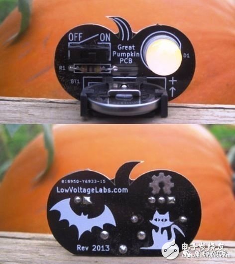
Note: The picture has nothing to do with the article!

1[Q] What should you pay attention to when wiring high-frequency signals?
Answer 1. Impedance matching of signal lines;
2. Space isolation from other signal lines;
3. For digital high frequency signals, the differential line effect will be better;
2[Q] In the layout, if the line is dense, there may be more vias, of course, it will affect the electrical performance of the board. How to improve the electrical performance of the board?
A For low frequency signals, the vias do not matter, and the high frequency signals minimize the vias. If the line is more, consider the multi-layer board;
3[Q] Is the decoupling capacitor added to the board as good as possible?
A decoupling capacitor needs to add the appropriate value at the appropriate position. For example, add the power supply port of your analog device and use different capacitor values ​​to filter out spurious signals at different frequencies.
4[Q] What is the standard for a good board?
The layout of the answer is reasonable, the power line power redundancy is sufficient, the high-frequency impedance impedance, and the low-frequency trace are simple.
5 [Q] How much influence does the through hole and blind hole have on the signal difference? What is the principle of application?
Answer The use of blind holes or buried holes is an effective way to increase the density of the multilayer board, reduce the number of layers and the size of the board, and greatly reduce the number of plated through holes. However, in comparison, the through hole is well realized in the process and the cost is low, so the through hole is used in the general design.
6[Q] When it comes to analog-digital hybrid systems, it is suggested that the electrical layer be divided, and the ground plane should be covered with copper. It is also suggested that the electric ground layer be divided, and different grounds are connected at the power source end, but the signal is reflowed. The path is far away. How to choose the appropriate method for specific applications?
A If you have a high frequency 20MHz signal line, and the length and number are more, then you need at least two layers to give this analog high frequency signal. One layer of signal lines, one layer of large area, and the signal line layer needs to make enough vias to the ground. The purpose of this is:
1. For analog signals, this provides a complete transmission medium and impedance matching;
2. The ground plane isolates the analog signal from other digital signals;
3, the ground circuit is small enough, because you have a lot of holes, the ground is a large plane.
7[Q] In the board, the signal input plug-in is on the leftmost edge of the PCB, and the MCU is on the right side. Then, in the layout, the regulated power supply chip is placed close to the connector (the power IC outputs 5V after a relatively long path). Arriving at the MCU), or placing the power IC to the center to the right (the 5V output of the power IC reaches the MCU is shorter, but the input power line goes through a longer PCB)? Or is there a better layout?
A. First of all, is your so-called signal input plug-in an analog device? If it is an analog device, it is recommended that your power supply layout should not affect the signal integrity of the analog part. Therefore, there are several points to consider (1) First of all, whether your regulated power supply chip is a relatively clean, low ripple power supply. For the power supply of the analog part, the requirements for the power supply are relatively high. (2) Whether the analog part and your MCU are a power supply. In the design of high-precision circuits, it is recommended to separate the power supply between the analog part and the digital part. (3) The power supply to the digital part needs to be considered to minimize the impact on the analog circuit.
8 [Q] In the application of high-speed signal chain, there are analog ground and digital ground for multiple ASICs. Is it ground split or undivided? What are the existing guidelines? Which effect is better?
A. So far, there is no conclusion. In general, you can check the manual of the chip. All of ADI's mixed-chip manuals recommend a grounding solution, some recommended for public ground and some for recommended isolation. It depends on the chip design.
9[Q] When should I consider the length of the line? If you want to consider using the isometric line, what is the difference between the lengths of the two signal lines? How to calculate?
Answer the difference line calculation idea: If you pass a sinusoidal signal, your length difference is equal to half of its transmission wavelength, and the phase difference is 180 degrees, then the two signals are completely offset. So the length difference at this time is the maximum value. By analogy, the signal line difference must be less than this value.
10 [Q] The serpentine line in the high speed, is it suitable for that situation? There are no disadvantages. For example, for differential traces, the two sets of signals are required to be orthogonal.
Answering a serpentine line, it has different functions because of different applications:
(1) If the serpentine trace appears in the computer board, it mainly acts as a filter inductor and impedance matching to improve the anti-interference ability of the circuit. Serpentine traces in computer motherboards are mainly used in some clock signals, such as PCI-Clk, AGPCIK, IDE, DIMM and other signal lines.
(2) In the general ordinary PCB board, in addition to the role of the filter inductor, it can also be used as an inductive coil of the radio antenna. For example, a 2.4G walkie-talkie is used as an inductor.
(3) The length of some signal wiring lengths must be strictly equal. The length of the high-speed digital PCB board is to keep the delay difference of each signal within a range, and to ensure the validity of the data read by the system in the same period ( When the delay difference exceeds one clock cycle, the data of the next cycle is misread). For example, HUBLink in the INTELHUB architecture has a total of 13 frequencies, and the frequency of 233MHz is required to be strictly equal in length to eliminate the hidden trouble caused by time lag. Winding is the only solution. Generally, the delay difference does not exceed 1/4 clock cycle, and the line delay difference per unit length is also fixed. The delay is related to line width, line length, copper thickness, and plate layer structure, but the line length increases the distributed capacitance and distributed inductance. To make the signal quality drop. Therefore, the clock IC pins are generally connected; "Terminal, but the serpentine trace does not act as an inductor. Conversely, the inductor will phase shift the higher harmonics in the rising edge of the signal, causing the signal quality to deteriorate, so It is required that the spacing of the serpentine line is at least twice the line width. The smaller the rise time of the signal, the more susceptible it is to the distributed capacitance and the distributed inductance.
(4) Serpentine traces function as an LC filter with distributed parameters in some special circuits.

11[Q] When designing a PCB, how to consider electromagnetic compatibility EMC/EMI, what needs to be considered? What measures are taken?
A good EMI/EMC design must take into account the location of the device, the layout of the PCB stack, the important online routing, and the choice of devices. For example, the position of the clock generator should not be close to the external connector. The high-speed signal should go as far as possible to the inner layer and pay attention to the characteristic impedance matching and the continuity of the reference layer to reduce the reflection. The slope of the signal pushed by the device is as small as possible to reduce the height. Frequency component, choose decoupling/bypass capacitors to pay attention to whether the frequency response meets the requirements to reduce power layer noise. In addition, pay attention to the return path of the high-frequency signal current so that the loop area is as small as possible (that is, the loop impedance is as small as possible) to reduce the radiation. It is also possible to divide the formation to control the range of high-frequency noise. Finally, the appropriate choice The grounding point of the PCB and the casing.
12[Q] Please ask the RF broadband circuit PCB transmission line design what needs attention? How to set the ground hole of the transmission line is appropriate, does impedance matching need to be designed by itself or with PCB processing manufacturers?
Answering this question requires consideration of many factors. For example, various parameters of the PCB material, the transmission line model finally established based on these parameters, the parameters of the device, and the like. Impedance matching is generally designed according to the information provided by the manufacturer.
13 [Q] When the analog circuit and the digital circuit coexist, half of them are the digital circuit part of the FPGA or the MCU, and the other half is the analog circuit part of the DAC and the related amplifier. There are many power sources of various voltage values, and the power supply that uses the voltage value used by both circuits of the digital and analog circuits, whether it is possible to use a common power supply, and what skills are there in the layout of the wiring and the magnetic beads. . ?
A general use is not recommended. This can be complicated to use and difficult to debug.
14[Q] Hello, what is the main basis for the selection of packages for resistors and capacitors when designing high-speed multilayer PCBs? Commonly used for those packages, can give a few examples.
Answer 0402 is commonly used in mobile phones; 0603 is commonly used for high-speed signals; the basis is that the smaller the package, the smaller the parasitic parameters. Of course, the same package of different manufacturers has great differences in high-frequency performance. It is recommended that you use high frequency components in critical locations.
15 [Q] Generally, in the design, is the double panel going to the signal line first or the ground line first?
Answer this to be considered comprehensively. Consider the trace when considering the layout first.
16[Q] What are the most important issues to be aware of when designing high-speed multilayer PCBs? Can you elaborate on the solution to the problem?
The most important thing to note is that the design of your layer is the signal line, power line, ground, and control line. How are you divided in each layer? The general principle is to ensure at least a single layer of analog and analog signals. A separate layer is also recommended for power supplies.
17[Q] Please ask when to use 2 layers, 4 layers, 6 layers, is there a strict technical limit? (Remove the volume) Is the frequency of the CPU or the frequency of its interaction with the external device data?
Answer The use of multi-layer boards can first provide a complete ground plane, and can provide more signal layers for easy routing. For the application of the CPU to control the external memory device, the frequency of interaction should be considered. If the frequency is high, the complete ground plane must be guaranteed. In addition, the signal line should preferably be of equal length.
18 [Q] How to analyze the influence of PCB layout on analog signal transmission, how to distinguish whether the noise introduced during signal transmission is caused by wiring or op amp device.
A. This is difficult to distinguish, only through the PCB wiring to minimize the wiring to introduce additional noise.
19[Q] I recently studied the design of PCB. For high-speed multi-layer PCB, it is appropriate to set the line width of power, ground and signal lines. What are the common settings? Can you give an example? For example, how to set the working frequency at 300Mhz?
A 300MHz signal must be impedance simulation to calculate the line width and the distance between the line and the ground; the power line needs to determine the line width according to the current line. When mixing the signal PCB, generally do not need "line", but use the entire plane, so To ensure that the loop resistance is minimal and that there is a complete plane below the signal line
20[Q] What kind of layout can I achieve the best heat dissipation?
There are three main sources of heat in the PCB: (1) heat generation of electronic components; (2) heat generation of P c B itself; and (3) heat from other parts. Among the three heat sources, the component generates the largest amount of heat, which is the main heat source, followed by the heat generated by the PCB board. The external heat input depends on the overall thermal design of the system, and is not considered for the time being. The purpose of the thermal design is to take appropriate measures and methods to reduce the temperature of the components and the temperature of the PCB, so that the system works properly at the right temperature. Mainly by reducing heat and speeding up heat dissipation.
21[Q] Can you explain the relationship between the line width and the size of the matching via?
Answering this question is very good. It is hard to say that there is a simple proportional relationship because his two simulations are different. One is a polygon transmission and the other is a circular transmission. You can find a perforation impedance calculation software on the Internet, and then keep the impedance of the via and the impedance of the transmission line consistent.
22[Q] In a common PCB circuit board with MCU control, but the requirements of high current and high speed signals are not very high, then whether the outermost edge of the PCB is covered with a ground wire will wrap the whole circuit board. Would it be better?
In general, it is enough to lay a complete land.
23[Q] 1, I know that the AD conversion chip should be connected to the single point of analog ground and digital ground, but what if there are multiple AD conversion chips on the board? 2. In a multi-layer circuit board, when a multi-channel switch (mulTIplexer) switches analog sampling, do you need to separate the analog part from the digital part like an AD conversion chip?
Answer 1. Several ADCs should be put together as much as possible. The analog ground digitally connects at a single point under the ADC. 2. Depending on the switching speed of the MUX and the ADC, the speed of the general ADC will be higher than the MUX, so it is recommended to place it below the ADC. Of course, for the sake of safety, you can also put a magnetic bead package under the MUX. When debugging, choose where to make a single point connection depending on the specific situation.
24 [Q] In the conventional network circuit design, some use several places together, and such usage? why? Thank you!
A is not very clear about your problem. There are certainly several types of ground for a hybrid system, and eventually they will be connected together at one point, the purpose of which is to equal potential. Everyone needs a common ground level for reference.
25 [Q] How to effectively deal with the analog part and the digital part of the PCB, analog ground and digital ground, thank you!
Answer The analog circuit and the digital circuit should be placed in separate areas so that the analog circuit is reflowed in the analog circuit area and the digital is in the digital area, so that the number does not affect the simulation. The starting point for analog ground and digital ground processing is similar, and the return of the digital signal cannot be allowed to flow to the analog ground.
26[Q] What are the differences in the design of ground lines for analog and digital circuits in PCB design? What issues need attention?
The main requirements of the analog circuit to the ground are: complete, small loop, and impedance matching. Digital signals are not particularly required if low frequency; if the speed is high, impedance matching and ground integrity are also considered.
27 [Q] Decoupling capacitors generally have two, 0.1 and 10. If the area is tight, how to place two capacitors, which one is better?
A should be designed according to the specific application and what chip
28[Q] Please ask the teacher, in the RF circuit, there will always be two signals of IQ. Do you need the same length of the two lines?
Answer Try to use the same in the RF circuit.
29 [Q] Is the design of the high-frequency signal circuit different from the ordinary circuit design? Can you briefly explain the layout design as an example?
A high-frequency circuit design should consider the influence of many parameters. Under high-frequency signals, many parameters that can be ignored by ordinary circuits cannot be ignored, so the transmission line effect may be considered.
30 [Q] High-speed PCB, how to deal with the avoidance of vias during the wiring process, is there any good advice?
A high-speed PCB, it is best to play less holes, increase the signal layer to solve the need to increase the need for vias.
31 [Q] How to choose the thickness of the power supply line in the PCB design? Is there any rules?
Answer can refer to: 0.15 & TImes; line width (mm) = A, also need to consider copper thickness
32 [Q] When the digital circuit and the analog circuit are on the same multi-layer board, should the analog ground and the digital ground be arranged on different layers?
A does not need to do this, but the analog circuit and the digital circuit are placed separately.
33[Q] Is it suitable to use up to several vias for general digital signal transmission? (Signal below 120Mhz)
A best not to exceed two vias.
34[Q] In the circuit with analog circuit and digital circuit, how to avoid mutual interference when designing PCB board?
A. Analog circuits are generally interfered if they match a reasonable amount of radiation. Sources of interference come from devices, power supplies, space, and PCBs; digital circuits are certainly sources of interference due to their large frequency components. The solution is generally reasonable device layout, power supply decoupling, PCB delamination, and if the interference characteristics are large or the analog part is very sensitive, a shield can be considered.
35[Q] For high-speed circuit boards, parasitic parameters may exist everywhere. In the face of these parasitic parameters, are we precise parameters and then eliminated, or empirical methods? How should this efficiency and performance be balanced?
A general analysis of the impact of parasitic parameters on circuit performance. If the impact cannot be ignored, it must be considered and eliminated.
36 [Q] What should you pay attention to when laying out the multi-layer board?
When answering the layout of the multi-layer board, because the power supply and the ground layer are in the inner layer, be careful not to have a suspended ground plane or power plane. Also, make sure that the vias hitting the ground are connected to the ground plane. Finally, it is important for some. The signal is added with some test points to facilitate measurement when debugging.
37 [Q] How to avoid crosstalk for high speed signals?
A can make the signal line farther away, avoid parallel lines, shield by laying or adding protection, and so on.
38[Q] I would like to ask the power plane in the multi-layer board design, but need to design the power plane in the double-layer board?
Answer is difficult, because your various signal lines are almost in the double layer layout.
39 [Q] What is the effect of the thickness of the PCB on the circuit? How is it generally selected?
The thickness of the answer is important when making impedance matching. The PCB manufacturer will ask if the impedance matching is calculated when the thickness is too high. The PCB manufacturer will make it according to your requirements.
40 [Q] The ground plane can make the signal minimum loop, but it will also generate parasitic capacitance with the signal line. How should this be chosen?
A depends on whether the parasitic capacitance has a non-negligible effect on the signal. If you can't ignore it, then rethink it.
41 [Q] LDO output as a digital power supply or analog power means that the digital and analog which first power supply output is good?
A If you want to use an LDO to provide power for digital and analog, it is recommended to connect the analog power supply first. After the analog power supply is filtered by the LC, it is a digital power supply.
42[Q] Please use magnetic beads between analog Vcc and digital Vcc, or should we use magnetic beads between analog ground and digital ground?
A. The analog VCC is LC filtered to obtain the digital VCC, and the magnetic beads are used between the analog ground and the digital ground.
43[Q] How to route differential signal lines such as LVDS?
A general need to pay attention: all wiring including the surrounding device placement, the ground plane needs to be symmetrical.
44 [Q] A good PCB design, you need to do as little as possible to emit electromagnetic radiation, but also to prevent external electromagnetic radiation to interfere with yourself, what measures should the circuit take to prevent external electromagnetic interference?
The best way to answer is to block and prevent external interference from entering. On the circuit, such as INA, you need to add RFI filter in front of INA to filter out RF interference.
45 [Q] How to solve the problem of transmission line effect when designing a PCB with a fast integrated circuit chip circuit with high clock frequency?
What chip is this fast integrated circuit chip? If it is a digital chip, generally do not have to consider. If it is an analog chip, it depends on whether the transmission line effect is large enough to affect the performance of the chip.
46[Q] Is there still a need for copper in a multi-layer PCB design? If copper is covered, which layer should it be connected to?
A If there is a complete ground plane and power plane inside, the top and bottom layers may not be copper.
47[Q] In the high-speed multi-layer PCB design, how to carry out impedance simulation generally, what software is used? Is there any problem that requires special attention?
A You can use MulTIsim software to simulate the resistor-capacitor effect.
48[Q] Some devices have thinner pins, but the traces on the PCB are thicker. Will the impedance mismatch be caused after the connection? If so how to solve it?
Answer to see what device. And the impedance of the device is generally given in the data sheet, generally has little to do with the thickness of the pin.
49 [Q] Differential lines generally need to be the same length. If it is difficult to achieve in LAYOUT, is there any other remedy?
Answers can solve the problem of equal length by taking the serpentine line. Now most PCB software can automatically take the same length line, which is very convenient.
50 [Q] When using the multimeter to measure the analog ground of the chip and the digital ground interface is conductive, so that the analog digital digital is not a multi-point connection?
The ground pins inside the chip are connected together. However, a connection is still required on the PCB. The ideal single-point grounding should be to understand the connection point location of the analog and digital parts of the chip, and then design the single-point connection location on the PCB to the analog and digital demarcation points of the chip.
51[Q] Due to the size limitation of the board, my circuit board uses two-sided patch soldering chip. A lot of vias are left on the board, and the signal line is also in the vicinity. Does the line interfere with the signal?
A If it is a low-speed digital signal, it should be a small problem. Otherwise it will definitely affect the quality of the signal.
52 [Q] When considering whether to do impedance matching, the digital line is to see if the total time exceeds 20% of the rising edge when the signal is transmitted to the reflection. If it exceeds, impedance matching is required. Does the analog line need impedance matching? How to think about it?
Answering the low frequency analog signal does not need to be matched. Of course, the analog signal of the radio frequency should also consider the matching problem.
53 [Q] Regarding the complete ground plane, on the board using the AD/DA chip, if the number of layers is relatively large, a complete analog ground and a complete digital ground can be provided; or both ground planes can be provided. Divide the analog ground and the digital ground separately. What are the advantages of both?
In general, the ground level will be paved. Unless it is a special case, such as the analog part of the board and the digital part are clearly separated, it can be easily distinguished.
54 [Q] When using magnetic beads or MECCA to connect digital and analog grounds, the frequency characteristics are used so that the high-frequency components in the digital ground do not affect the analog ground, and the two levels are equal. Then, 0ohm resistors connect digital, analog ground, and sometimes only use a small piece of copper connection, can you analyze it?
The equivalent circuit of the magnetic bead is equivalent to the band-stopper, which only significantly suppresses the noise of a certain frequency. When using it, it is necessary to estimate the noise frequency in advance so that the appropriate model can be selected. For frequencies that are uncertain or unpredictable, the beads do not match. The 0 ohm resistor is equivalent to a very narrow current path, which effectively limits the loop current and suppresses noise. The resistor has an attenuation in all frequency bands (0 ohm resistor also has impedance), which is stronger than the magnetic beads. The copper skin is similar to a 0 ohm resistor.
55[Q] How to avoid the noise introduced during wiring?
Answer The digital ground and the analog ground should be grounded at a single point, otherwise the digital ground return will cause interference to the analog circuit through the analog ground.
56[Q] How does the PCB prevent the interference of the abrupt signal such as PWM on the analog signal (such as an op amp), and how to test the interference (radiation interference or conducted interference)? In addition to the layout and wiring need to pay attention, is there any other way to suppress (except the means of shielding?
A. From the several interfaces of the op amp, the input should prevent spatial coupling interference and PCB crosstalk (layout improvement); the power supply requires different capacitance decoupling capacitors. The test can use the oscilloscope's probe to test the position mentioned above to determine where the interference comes from. If the PWM signal is converted to DC control voltage through low-pass filtering, it can be considered to filter, or a small capacitor connected in parallel to make the PWM waveform round and reduce high-frequency components.
57[Q] Excuse me, in the circuit board, an ARM or FPGA often connects a lot of RAM, FLAH devices, what are the connections between these main chips and these memories, what is the number of vias? Is it restricted? What is the size of the via hole commonly used in digital signals? Does the size of the via aperture have a large effect on the signal?
Answer If the speed is greater than 100MHz, it is better not to exceed more than two vias on one signal line. The vias should not be too small. Generally, the aperture of 10 mils can be used.
58 [Q] When the double panel of the cloth (high frequency is), the fewer the vias when the top layer is connected to the bottom layer, the better? So how to put a hole is more reasonable?
Answering the hole is for the signal line. If it is the ground via, more appropriate will reduce the ground loop and impedance. The principle of putting it in is to enter the device.
59 [Q] What should I pay attention to LVDS signal wiring? How to route?
A parallel isometric
60[Q] Is the data line parallel wiring for mutual interference?
Answer and walk the line to pay attention to the line-to-line spacing to prevent crosstalk.
61 [Q] In a 4-layer board, there is an entire acquisition system with analog amplification, digital acquisition, and MCU. After the cloth is laid, how to measure the input impedance of the system, how to match the input impedance of the system and the sensor, how to match, there is no relevant design principle.
A don't know how high your analog signal is. If it is not high, you don't need impedance matching. Impedance matching can use some simulation software to calculate the impedance of the PCB. For example APPCAD. The impedance of the device can be queried by the manual.
62[Q] I often see a lot of holes on the PCB. The more holes, the better? Is there any rules?
A: No. To minimize the use of vias, consider reducing the effects of vias on the circuit when you have to use vias.
63 [Q] There is inevitably a cross-plane phenomenon when wiring a multi-layer board. Our current cooking is to give priority to the differential line without crossing the plane when cutting the plane. But once I thought the teacher’s statement was that the single-ended could not cross, and the difference was not so strict. Ask the teacher about this.
Answer that the single-ended and differential signals have to flow back after crossing the ground plane. If the reflow returns around a large circle, it will induce more interference. If the noise on the difference line is the same, it will cancel each other, so there is Certainly reasonable.
64 [Q] How to distinguish between digital ground and analog ground in high-speed multilayer PCB design? Is it connected as described in the device data sheet?
A high-speed design does not need to be divided into digital ground and analog ground.
65 [Q] How to consider the fuse current of PCB trace? ? When the PCB traces, the current will blow, what factors are related?
Answer 0.15 & TImes; line width (mm) = A, then the maximum current. It is not possible to use the blown current to make a budget when designing. This is the cross-sectional area of ​​the copper wire.
66[Q] Please ask what protection is needed in the signal input and output interface and power input interface? When the power supply is 220V input to DC, what protective measures are needed in actual application?
Answer TVS tube, fuses are necessary on the power supply. If the signal is used, it is necessary to add a TVS tube and a diode to protect the analog circuit from the presence of a large voltage.
67[Q] See the 45-degree angle and the arc when the PCB board is bent. What are the advantages and disadvantages? How to choose?
A. From the perspective of impedance matching, both lines can be made to match the corners. However, rounded corners may not be well processed.
68[Q] If the size is limited in the high-frequency trace, what are the most commonly used routing methods or reasonable routing methods? For example, snake-shaped lines, can you?
Bad answer, will introduce more parasitic parameters
69[Q] I ask the key input model when using the instrumentation amplifier. I still need copper over the device layer. I have already covered the copper on the bottom layer of the device. There is also the feedback resistance of the instrumentation amplifier. I use the in-line, the lead wire is long, and the temperature drift and accuracy of the patch are not up to the requirements. How to deal with it.
A general method of placing the chip data will have a recommended layout method and diagram, you can refer to. It is necessary to ensure that the leads are short and thick. It is better to choose the low-precision resistor of the chip or the high-precision resistor. It depends on the result of the specific debugging.
70[Q] The PCB software can be automatically routed, but is the position layout of the device to be manually placed?
A best place and route are done manually.
71[Q] When doing PCB board making, is there any special regulation for PCB material selection or how to choose materials? I am currently working on a high-frequency signal board. What is the best choice for a PCB board?
A. The high-frequency circuit board substrate currently used is a fluorine-fluoride dielectric substrate, such as polytetrafluoroethylene (PTFE), which is usually called Teflon, and is usually applied at 5 GHz or higher. When you are doing the board, you can explain it with the PCB manufacturer.
72[Q] I am a beginner in PCB design. I want to know what is the selection rule for the coupling capacitor? How is the size of the value calculated?
A general situation, for the power generation part, to use 10u and 0.1u capacitor decoupling, we must consider both high frequency and low frequency decoupling; for other originals are generally 0.1u capacitor decoupling in the power supply part.
73[Q] What is the attenuation of a 5khz pulse signal after walking 20cm long and 10mil wide on the board?
A. Different materials have different parasitic parameters of the PCB, which can be calculated according to the parasitic parameters you use.
74[Q] What are the requirements for the distance between the microstrip line and the ground plane in the high frequency? For example, greater than 1mm. Still not much demand, as long as it is almost enough? Still have to calculate by coplanar waveguide?
Answer must be calculated using the impedance simulation of the coplanar waveguide or microstrip line.
75 [Q] How to route to minimize the crosstalk of high frequency signals between lines?
Answering high frequency signals will reduce reflections and also reduce radiation.
76[Q] I would like to ask DC-DCConvertIC, need to connect to the ground plane under the IC, connect to the ground plane through Via, what is the number of Via holes and how much influence? .
The answer can generally be designed according to the reference design. Due to the large current, a certain number of Vias may be required.
77[Q] When the impedance is matched, if the impedance value given by the pin is complex, that is, both the impedance part and the reactance part, what is the impedance matching? Does light take into account the resistance part?
A. Consider conjugate matching and offset the imaginary part of the impedance.
78[Q] Is it better to concentrate parameters and distribution parameters in high frequencies? How to choose these two methods is more appropriate? Thank you!
The answer distribution method has higher precision, but it is more complicated; the lumping method is relatively simplified, but there is a certain error.
79[Q] What are the requirements for the distribution of the vias connecting the upper and lower copper plates?
Generally speaking, in order to improve connectivity, there should be no requirements for each.
80[Q] How to balance the parasitic inductance and parasitic capacitance at the input of the amplifier in IF applications?
In general, parasitic inductance and capacitance have little effect on the IF circuit and can be ignored. Just make sure you don't introduce large parasitic capacitance and inductance values.

81[Q] How can I effectively reduce the interference effects between circuit components and how the amplifier is laid out to minimize the introduction of ripple?
The principle of reducing interference is:
1. Reduce the radiation end;
2. Strengthen the isolation, shielding and withdrawal of the interference;
The principle of ripple reduction is also
1. Reduce the ripple output of the switching power supply;
2. Sufficient decoupling filtering;
82 [Q] When the 6-layer design, the layer distribution skills, those lines have to go to the middle layer?
Answer your design. The principle is to ensure that the analog signal line and the analog ground have two separate layers.
83 [Q] When the analog ground is connected to the digital ground, is the method used to connect a suitable magnetic bead to the analog ground in the digital ground? How to choose this magnetic bead? Thank you!
The magnetic beads mainly play the role of isolating high-frequency noise. Different bead filter frequencies are different, so it is necessary to select the appropriate device according to the noise on the board.
84[Q] What should I pay attention to for signal layouts above 5G?
Answering both the transmission line effect and the parasitic effects, as well as the EMI problem.
85 [Q] When there is a high-speed logic device in the circuit, what is the maximum wiring length?
Answer wiring is not afraid of long, afraid of asymmetry or a relatively large difference, so it is easy to cause wrong logic due to delay
86[Q] In a high-speed digital circuit board, there are multiple power supplies with different voltage values. When laying the power plane, should you use multi-layer power planes or separate layouts on the same power plane?
A can be multiple voltages on one plane, pay attention to the isolation. It is also possible to separate the most important power supply by one layer, so that it is not interfered by other power sources.
87[Q] When the difference line is taken, due to space constraints, it cannot be completely equidistant. Is it equidistant or equal?
Answer length can guarantee impedance matching, but unequal distance actually affects differential matching and requires simulation test.
88[Q] How to reduce electromagnetic interference in PCB layout? Which other modules should be closer to the main control chip? Thank you!
Answer For the main controller, the main signal is transmitted, so the analog and power parts should be away from the controller; for reducing electromagnetic interference, attention should be paid to matching, decoupling, place and route, layering, etc. It is recommended to refer to some information.
89 [Q] When considering signal integrity, if you only know that the frequency of the digital chip is 1 GHz, it is generally estimated that his rise time is 1/10 of the period, that is, 0.1 ns. What is the basis?
A This is a general principle and the speed of the edge depends on the speed of the device's output. If it is too slow, it will affect the judgment. Faster chip technology can't be achieved.
90[Q] Hello, may I ask the ARM chip to improve the anti-interference of the power supply, except that the TVS tube is connected to the power input terminal, the input pin of the power input terminal should be connected to the inductor better, or the magnetic beads are better.

A will generally use magnetic beads.
91[Q] Hello, pcb board online can not simulate, that is, how to verify the board has no problem, thank you?
A. Some PCB software can do some trace inspection and integrity analysis, such as CADENCE
92 [Q] Some people in the pcb wiring when the signal input and output end string of a resistor to terminate, this role is large? How to choose this resistor? Which places need to do this? Thank you!
Answer this depends on the role of series resistors, some of which are used to limit current, and some may be impedance matching.
93[问] 对影å“电æºçš„高速脉冲串有什么好的抑制方案或者æˆæ¯”较系统的处ç†æ–¹æ³•å—?
ç”æ‚¨æ‰€è°“çš„é«˜é€Ÿè„‰å†²ä¸²ï¼Œæ— éžå°±æ˜¯ä¸åŒé¢‘率的干扰信å·ï¼Œé‡‡ç”¨ä¸åŒå€¼çš„电容退å¶ã€‚
94 [问] 高速PCB对æ¿æ有什么特殊è¦æ±‚没有?
ç”高频电路对PCBæ料有è¦æ±‚.在高频下è¦è€ƒè™‘ä¼ è¾“çº¿æ•ˆåº”
95[问] 关于信å·çº¿çš„阻抗匹é…,请作点介ç»å’Œä½œæ³•ï¼Ÿ
ç”频率较低场åˆï¼Œéœ€è¦è€ƒè™‘ä¿¡å·çº¿çš„宽度和电æµçš„承载能力的关系,高频时,需è¦è€ƒè™‘匹é…ç‰é•¿ç‰é—®é¢˜ã€‚
96[问] 高频信å·çº¿çš„抗干扰措施有哪些?布线时应注æ„哪些方é¢ï¼Ÿ
ç”这个问题比较宽泛,很难一两å¥è¯è¯´æ¸…楚。有很多相关资料å¯ä»¥å‚考。
97[问] 为什么高速信å·ä¸ç”¨åˆ†æ•°å—和模拟地?
ç”å› ä¸ºé©±åŠ¨å™¨ç«¯å¯ä»¥è°ƒæ•´è¾“出相ä½å·®ï¼ŒPCB布局好了å†è°ƒæ•´å°±å¾ˆéš¾äº†ï¼ŒæŽ¥æ”¶ç«¯ç›´æŽ¥è¾“å…¥äº†ï¼Œæ— æ³•è°ƒæ•´ã€‚
98[问] 关于差分线的ç‰é•¿è¡¥å¿ï¼Œæ‚¨ä¸ºä½•å°±ç›´æŽ¥å»ºè®®åœ¨é©±åŠ¨å™¨ç«¯è¡¥å¿å‘¢ï¼Ÿèƒ½è§£é‡Šä¸€ä¸‹å—?EricBogatin的书ä¸ä¹Ÿåªæ˜¯ç»™å‡ºç»“è®ºï¼Œä½†æ— è§£é‡Šã€‚
ç”驱动端有些芯片有调整功能,PCB线设计好ä¸å®¹æ˜“改了,接å—端直接输入一般都没有时延调整的功能。
99[问] 在高频选用制æ¿æ料时,介电常数是ä¸æ˜¯è¶Šå°è¶Šå¥½å‘¢ï¼Ÿ Thank you!
ç”æ„味ç€å¯„生电容å°ï¼Œç„¶è€Œå¯¹äºŽä¿¡å·çº¿ç‰¹å¾é˜»æŠ—的设计时对介电常数是有è¦æ±‚的,ä¸èƒ½ä¸€æ¦‚而论。
100[问] 多大频率的晶振è¦è€ƒè™‘MCU与晶振间的走线方å¼ï¼Ÿ
ç”晶振与MCU应尽é‡é 近,用最çŸçš„直线连接。
101 [问] 开关电æºè¿‡æ¥çš„ç›´æµç”µä¸Šé¢å¸¦æœ‰100mvå·¦å³çš„噪声,应该如何有效地滤除?
ç”å¯ä»¥è€ƒè™‘åŠ ä¸€çº§è°ƒåˆ¶å™¨LDO产å“稳定电æºï¼Œæˆ–者考虑适当的去耦电容滤除纹波。
102[问] 模拟电æºæ˜¯å¦ä¹Ÿå¯ä»¥é“ºå¹³é¢ï¼Œæ˜¯å¦å’Œåœ°çš„作用相åŒï¼Ÿ
ç”电æºå½“然å¯ä»¥é“ºå¹³é¢ã€‚è‹¥ä¸èƒ½é“ºå¹³é¢ï¼Œç”µæºçº¿è¦å°½é‡ç²—。
103[问] 请问专家,两层电路æ¿çš„覆铜,什么时候选择两é¢å‡è¦†ï¼Œä»€ä¹ˆæ—¶å€™ä»…选择一é¢è¦†é“œå‘¢ï¼Ÿ
ç”如果能ä¿è¯ä¸€é¢æ˜¯å…¨åœ°å¹³é¢çš„è¯ï¼Œå¯ä»¥åªé“ºä¸€å±‚。
104[问] 请问在高频(1GHz以上)æ¿çš„设计ä¸ï¼Œè¿‡å”的大å°åŠè¿‡å”é—´è·æœ‰ä»€ä¹ˆè¦æ±‚?阻抗匹é…时需è¦è€ƒè™‘åˆ°çš„å› ç´ æœ‰å“ªäº›ï¼Ÿæ¿æ需è¦æ³¨æ„么?差分走线与地平é¢çš„è·ç¦»æœ‰ä»€ä¹ˆæ³¨æ„事项?
ç”如何需è¦ç»¼åˆè€ƒè™‘ä»¥ä¸ŠæŒ‡æ ‡ï¼Œå»ºè®®åšæ•´ä½“的电路仿真和调试,寄生效应会影å“仿真效果,需è¦è¿›è¡Œåå¤éªŒè¯å’Œå°è¯•ã€‚
105 [问] 敷铜的9个注æ„点
ç”所谓覆铜,就是将PCB上闲置的空间作为基准é¢ï¼Œç„¶åŽç”¨å›ºä½“铜填充,这些铜区åˆç§°ä¸ºçŒé“œã€‚敷铜的æ„义在于,å‡å°åœ°çº¿é˜»æŠ—,æ高抗干扰能力;é™ä½ŽåŽ‹é™ï¼Œæ高电æºæ•ˆçŽ‡ï¼›ä¸Žåœ°çº¿ç›¸è¿žï¼Œè¿˜å¯ä»¥å‡å°çŽ¯è·¯é¢ç§¯ã€‚
敷铜方é¢éœ€è¦æ³¨æ„那些问题:
1.如果PCB的地较多,有SGNDã€AGNDã€GND,ç‰ç‰ï¼Œå°±è¦æ ¹æ®PCBæ¿é¢ä½ç½®çš„ä¸åŒï¼Œåˆ†åˆ«ä»¥æœ€ä¸»è¦çš„“地â€ä½œä¸ºåŸºå‡†å‚考æ¥ç‹¬ç«‹è¦†é“œï¼Œ æ•°å—地和模拟地分开æ¥æ•·é“œè‡ªä¸å¤šè¨€ï¼ŒåŒæ—¶åœ¨è¦†é“œä¹‹å‰ï¼Œé¦–å…ˆåŠ ç²—ç›¸åº”çš„ç”µæºè¿žçº¿ï¼š5.0Vã€3.3Vç‰ç‰ï¼Œè¿™æ ·ä¸€æ¥ï¼Œå°±å½¢æˆäº†å¤šä¸ªä¸åŒå½¢çŠ¶çš„多å˜å½¢ç»“构。
2.对ä¸åŒåœ°çš„å•ç‚¹è¿žæŽ¥ï¼Œåšæ³•æ˜¯é€šè¿‡0欧电阻ç£ç 有很高的电阻率和ç£å¯¼çŽ‡ï¼Œä»–ç‰æ•ˆäºŽç”µé˜»å’Œç”µæ„Ÿä¸²è”,但电阻值和电感值都éšé¢‘率å˜åŒ–。 He has better high-frequency filtering characteristics than ordinary inductors and resistive at high frequencies, so it can maintain high impedance over a wide frequency range, thus improving the frequency modulation filtering effect. As a power supply filter, an inductor can be used.ç£ç 的电路符å·å°±æ˜¯ç”µæ„Ÿä½†æ˜¯åž‹å·ä¸Šå¯ä»¥çœ‹å‡ºä½¿ç”¨çš„是ç£ç 在电路功能上,ç£ç 和电感是原ç†ç›¸åŒçš„,åªæ˜¯é¢‘率特性ä¸åŒç½¢äº†ï¼Œ ç£ç 由氧ç£ä½“组æˆï¼Œç”µæ„Ÿç”±ç£å¿ƒå’Œçº¿åœˆç»„æˆï¼Œç£ç 把交æµä¿¡å·è½¬åŒ–为çƒèƒ½ï¼Œç”µæ„ŸæŠŠäº¤æµå˜å‚¨èµ·æ¥ï¼Œç¼“慢的释放出去。 Magnetic beads have a great hindrance to high-frequency signals. The general specification is 100 ohms/100mMHZ, which is much smaller than the inductor at low frequencies.
3.晶振:电路ä¸çš„晶振为一高频å‘å°„æºï¼Œåšæ³•æ˜¯åœ¨çŽ¯ç»•æ™¶æŒ¯æ•·é“œï¼Œç„¶åŽå°†æ™¶æŒ¯çš„外壳å¦è¡ŒæŽ¥åœ°ã€‚
4.å¤å²›ï¼ˆæ»åŒºï¼‰é—®é¢˜ï¼Œå¦‚果觉得很大,那就定义个地过å”æ·»åŠ è¿›åŽ»ä¹Ÿè´¹ä¸äº†å¤šå¤§çš„事。
5.在开始布线时,应对地线一视åŒä»ï¼Œèµ°çº¿çš„时候就应该把地线走好,ä¸èƒ½ä¾é 于铜åŽé€šè¿‡æ·»åŠ 过å”æ¥æ¶ˆé™¤ä¸ºè¿žæŽ¥çš„åœ°å¼•è„šï¼Œè¿™æ ·çš„æ•ˆæžœå¾ˆä¸å¥½ã€‚
6.在æ¿å上最好ä¸è¦æœ‰å°–的角出现(<=180åº¦ï¼‰ï¼Œå› ä¸ºä»Žç”µç£å¦çš„角度æ¥è®²ï¼Œè¿™å°±æž„æˆçš„一个å‘射天线ï¼å¯¹äºŽå…¶ä»–总会有一影å“çš„åªä¸è¿‡æ˜¯å¤§è¿˜æ˜¯å°è€Œå·²ï¼Œæˆ‘建议使用圆弧的边沿线。
7.多层æ¿ä¸é—´å±‚的布线空旷区域,ä¸è¦æ•·é“œã€‚ Because it is very difficult for you to make this copper "good grounding"
8.设备内部的金属,例如金属散çƒå™¨ã€é‡‘å±žåŠ å›ºæ¡ç‰ï¼Œä¸€å®šè¦å®žçŽ°â€œè‰¯å¥½æŽ¥åœ°â€ã€‚
9.三端稳压器的回æµé¢ç§¯ï¼Œå‡å°ä¿¡å·å¯¹å¤–的电ç£å¹²æ‰°ã€‚
ã€å¼ 飞硬件电路全集】电å工程师必备å®å…¸ï¼Œå·²æœ‰è¶…过10W+电å工程师å¦ä¹ ï¼

ç«‹å³å¼€å§‹æ‚¨çš„硬件电路å¦ä¹ ä¹‹è·¯ï¼ >>点击查看
Switch & Socket,Sockets And Switches,Brass Plug Sockets,Light Switches And Sockets
WENZHOU TENGCAI ELECTRIC CO.,LTD , https://www.tengcaielectric.com
